|
 JWST JWST
JWST (James Webb Space Telescope)
Concept Launch Observatory Mission Status Sensor Complement Spacecraft Bus and Sunshield
Spinoff Technologies References
JWST is an orbiting optical observatory and a key element in NASA's Origins Program, optimized for observations in the infrared region of the electromagnetic spectrum. It is considered the successor mission of HST (Hubble Space Telescope) while operating over a different spectral range. At the NIR and MWIR wavelengths, it benefits from operating at intrinsically lower backgrounds than any comparably sized telescope on the ground. JWST, previously known as NGST (Next Generation Space Telescope), will be the premier space facility for astronomers in the decade following its launch. The overall objectives are to study the first stars and galaxies after the big bang. Major science goals (themes) of the mission are to find answers to the following questions: 1) 2)
• What is the shape of the Universe?
• How do galaxies evolve?
• How do stars and planetary systems form and interact?
• How did the Universe built up its present chemical/elemental composition?
• What is the nature of dark matter?
The radiation from the very distant objects to be observed is practically all in the infrared region. Many of the early events happened when the Universe was between 1 million and 1 billion years old, a period that is not known to earthlings (the dark ages of the Universe). To accomplish the goals of the science themes, the main JWST design requirement calls for the detection of objects up to 400 times fainter than those observable by current ground-based or spaceborne observatories.
Historical background: Large next-generation projects with high-performance observation requirements take about two decades (and more) from first studies to launch. Initial planning for the new mission started in 1989 (visions, conceptual studies). The goal was to have a successor mission for HST ready for launch well before 2010.
In the mid-1990s, a telescope design with an 8 m aperture was considered. The challenge was to come up with a lower cost for the large telescope than for previous much smaller space telescopes. This involved conceptual studies by industry. In 1996, a committee report was written, based on these studies: "Next Generation Space Telescope, Visiting a Time When Galaxies Were Young." This report established also a roadmap to NGST activities, defining the new building blocks and to search for enabling technologies and concepts - in particular in the fields of large-aperture lightweight mirrors that are actively controlled, of advanced detector designs, of suitable cooling techniques for all critical components, and of precision metrology to achieve the goal of measuring ultra precise stellar positions.
A broad range of talent on a national and international level and from many institutions, academia and industry was directly involved in the NGST detailed definition phase (Phase A) including simulations and feasibility studies. In 1997, an ad hoc Science Working Group was formed which came up with thematic science goals and developed a so-called "Design Reference Mission" (DRM), representing a hypothetical suite of key science observing programs [stating the expected physical properties (number density and brightness), the desired observation modes (wavelength band, spectral resolution, number of revisits), and a minimum operational life of 2.5 years to complete the mission] for NGST - which provided a yardstick for technology testing. DRM was and is the primary tool against which any JWST architectures are being measured. The shear complexity of the project and the performance requirements demanded a technology development and validation strategy to address and demonstrate a critical path to a workable design of the mission. 3) 4) 5) 6)
In 2000/1, the NGST project experienced a rescoping of the telescope size (from 8 m aperture to 6.5 m) to keep projected costs in bounds. There were also some technology maturity uncertainties.
The project started in 2002 with a Mission Definition Review. NASA began to realize that the critical technologies had reached a level of sufficient maturity to justify a go-ahead with the next phase of the project.
In September 2002, NASA renamed NGST to JWST (James Webb Space Telescope) in honor of James E. Webb (1906-1992), NASA's second administrator during the Apollo Program of the 1960s (1961-1968). At the same time in Sept. 2002, NASA awarded the prime contract of the JWST observatory development (spacecraft, telescope, integration and testing) to Northrop Grumman Space Technology (formerly TRW) of Redondo Beach, CA.
In the fall of 2003 ICR(Initial Confirmation Review) was given, starting the Phase B of the JWST project. The C/D Phase started in 2008.
The CDR (Critical Design Review) of the JWST (James Webb Space Telescope) is planned for December 2013 (Ref. 28).
Project partners: NASA leads an international partnership in the joint JWST mission that includes ESA (European Space Agency) and CSA (Canadian Space Agency). Both agencies (ESA, CSA) collaborated in the JWST project already at an early planning stage (1996). Aside from instrument contributions, ESA will also launch the JWST spacecraft on an Ariane 5 launcher as agreed to with NASA. NASA/GSFC is managing the JWST project, while STScI (Space Telescope Science Institute) of Baltimore, MD, is responsible for JWST science and mission operations, as well as ground station development (STScI is the same organization that is operating the Hubble Space Telescope). A formal JWST and LISA (Laser Interferometer Space Antenna) cooperation agreement between NASA and ESA was signed on June 18, 2007 at the International Paris Air Show at Le Bourget, France. 7) 8) 9) 10) 11)
A most interesting and valuable side effect of the technology development effort for JWST is that these new technologies will also be available to many other space projects (astronomy, space science, Earth observation, etc.) providing potentially a quantum step in observation performance.
Mission concept
The JWST mission concept is an ambitious and most challenging development program, requiring a lot of innovative technology introduction as well as conceptual breakthroughs on various levels to meet the proposed observational performances. The objectives of the science themes can only be met by a combination of a large-aperture telescope in space (6.5 m φ ), a very low detection temperature to eliminate noise, and an ideal observing environment (elimination of stray light).
The observatory will be shielded from the sun and Earth by a large deployable sunshade, the entire telescope assembly will be passively cooled to about 37 K, giving JWST exceptional performance in the near-infrared and mid-infrared wavebands. The baseline wavelength range for the instrumentation is 0.6 - 28 µm, and the telescope will be diffraction-limited above 2 µm. The sensitivity of the telescope will be limited only by the natural zodiacal background, and should exceed that of ground-based and other space-based observatories by factors of 10 to 100,000, depending on the wavelength and type of observation. The JWST observatory will have a 5 year design life (with a goal of 10 years of operations) and will not be serviceable by astronauts (as is Hubble). The total mass of JWST at launch is estimated to be 6,500 kg.
Like Hubble, the JWST will be used by a broad astronomical community to observe targets ranging from objects within our Solar System to the most remote galaxies seen during their formation in the early universe.
Major enabling technologies are:
• Large deployable and lightweight beryllium mirrors (a folding 6.5 meter mirror made up of 18 individual segments, adjustable by cryogenic actuators). To fit inside the launch vehicle, the large space telescope prime mirror must be folded in sections for launch, then unfolded (deployed) precisely into place after launch, making it the first segmented optical system deployed in space.
• Deployment of large structures. Once in space, the multilayer sunshield that was folded over the optics during launch will deploy to its full size and keep the telescope shadowed from the sun.
• Introduction of MEMS technology to the microshutter system of the NIRSpec instrument. The programmable microshutters to allow object selection for the spectrograph.
Overview of payload instruments:
• NIRCam (Near-Infrared Camera), funded by NASA with the University of Arizona as prime contractor. CSA is participating in the development of the NIRCam instrument.
• NIRSpec (Near-Infrared multi-object Spectrograph), funded by ESA with EADS Astrium GmbH as prime contractor (the detector arrays and a micro-shutter are supplied by NASA/GSFC)
• MIRI (Mid-Infrared Camera-Spectrograph) a joint instrument of JPL and ESA. The instrument (about 50%) is being provided by ESA member states, coordinated but not funded by ESA.
• FGS (Fine Guidance Sensor) with TFI (Tunable Filter Imager), funded by CSA (Canadian Space Agency)

Figure 1: Photometric performance of JWST instruments as compared to those of current observatories (image credit: STScI)
Legend to Figure 1: Plotted is the faintest flux for a point source that can be detected at 10 sigma in a 104 s integration. The fluxes are given in Janskies as well as AB magnitudes. 12)

Figure 2: Comparison of JWST light gathering power vs spectral range with Hubble and Spitzer telescopes (image credit: STScI) 13)
Launch: On Saturday, December 25 (Christmas), 2021 at 9:20 am local time (12:20 UTC), an Ariane 5 rocket lifted off from the Guiana Space Center, Europe's Spaceport in Kourou, French Guiana (South America), injecting the Webb Space Telescope, developed by NASA in partnership with ESA and the Canadian Space Agency (CSA), into its transfer orbit. The telescope was successfully separated from the launcher 27 minutes after liftoff. 14) 15)
The telescope now embarks on a voyage lasting 29 days to reach the second Lagrange point.
• On the third day, the heat shield will begin to deploy. On the eleventh day, the secondary mirror will begin positioning.
• Between the 13th and 14th day, the primary mirror, comprising 18 hexagonal segments and measuring 6.5 meters in diameter, will be assembled.
• The telescope is slated to arrive at its final destination, 1.5 million kilometers from Earth, approximately 29 days after launch.
The space agencies of the United States (NASA), Europe (ESA) and Canada (CSA) teamed up to develop this telescope. Europe played an important role in this mission, with ESA providing the launch onboard Ariane 5, as well as the Nirspec spectrometer built by Airbus. The astrophysics department of the Saclay-based CEA (French Alternative Energies and Atomic Energy Commission) and the Paris Observatory designed the MIRI camera. This is the most ambitious telescope ever sent into space.
"Today's launch is the mission of the decade," said Stephane Israël, Chief Executive Officer of Arianespace, "one that demonstrates the reliability of Arianespace's launch services in the eyes of the international space community. It's a great honor for us to have been chosen for this launch, which will enable humanity to take a giant step forward in its knowledge of the Universe. The mission demanded 20 years of preparation hand in hand with NASA. It's the third launch we have performed for the American space agency, clearly illustrating the advantage of large-scale international collaboration in space. I would like to thank ESA, NASA and CSA for entrusting us with their invaluable payload. To launch on Christmas morning 42 years after the takeoff of the first Ariane from this same Kourou site ... What a great end of year present for the space community gathered today for this launch.
NASA: A joint effort with ESA (European Space Agency) and the Canadian Space Agency, the Webb observatory is NASA's revolutionary flagship mission to seek the light from the first galaxies in the early universe and to explore our own solar system, as well as planets orbiting other stars, called exoplanets. 16)
"The James Webb Space Telescope represents the ambition that NASA and our partners maintain to propel us forward into the future," said NASA Administrator Bill Nelson. "The promise of Webb is not what we know we will discover; it's what we don't yet understand or can't yet fathom about our universe. I can't wait to see what it uncovers!"
Ground teams began receiving telemetry data from Webb about five minutes after launch. The Arianespace Ariane 5 rocket performed as expected, separating from the observatory 27 minutes into the flight. The observatory was released at an altitude of approximately 870 miles (1,400 km). Approximately 30 minutes after launch, Webb unfolded its solar array, and mission managers confirmed that the solar array was providing power to the observatory. After solar array deployment, mission operators will establish a communications link with the observatory via the Malindi ground station in Kenya, and ground control at the Space Telescope Science Institute in Baltimore will send the first commands to the spacecraft.
Engineers and ground controllers will conduct the first of three mid-course correction burns about 12 hours and 30 minutes after launch, firing Webb's thrusters to maneuver the spacecraft on an optimal trajectory toward its destination in orbit about 1 million miles from Earth.
"I want to congratulate the team on this incredible achievement – Webb's launch marks a significant moment not only for NASA, but for thousands of people worldwide who dedicated their time and talent to this mission over the years," said Thomas Zurbuchen, associate administrator for the Science Mission Directorate at NASA Headquarters in Washington. "Webb's scientific promise is now closer than it ever has been. We are poised on the edge of a truly exciting time of discovery, of things we've never before seen or imagined."
The world's largest and most complex space science observatory will now begin six months of commissioning in space. At the end of commissioning, Webb will deliver its first images. Webb carries four state-of-the-art science instruments with highly sensitive infrared detectors of unprecedented resolution. Webb will study infrared light from celestial objects with much greater clarity than ever before. The premier mission is the scientific successor to NASA's iconic Hubble and Spitzer space telescopes, built to complement and further the scientific discoveries of these and other missions.
"The launch of the Webb Space Telescope is a pivotal moment – this is just the beginning for the Webb mission," said Gregory L. Robinson, Webb's program director at NASA Headquarters. "Now we will watch Webb's highly anticipated and critical 29 days on the edge. When the spacecraft unfurls in space, Webb will undergo the most difficult and complex deployment sequence ever attempted in space. Once commissioning is complete, we will see awe-inspiring images that will capture our imagination."
The telescope's revolutionary technology will explore every phase of cosmic history – from within our solar system to the most distant observable galaxies in the early universe, to everything in between. Webb will reveal new and unexpected discoveries and help humanity understand the origins of the universe and our place in it.
NASA Headquarters oversees the mission for the agency's Science Mission Directorate. NASA's Goddard Space Flight Center in Greenbelt, Maryland, manages Webb for the agency and oversees work on the mission performed by the Space Telescope Science Institute, Northrop Grumman, and other mission partners. In addition to Goddard, several NASA centers contributed to the project, including the agency's Johnson Space Center in Houston, Jet Propulsion Laboratory in Southern California, Marshall Space Flight Center in Huntsville, Alabama, Ames Research Center in California's Silicon Valley, and others.

Figure 3: The James Webb Space Telescope lifted off on an Ariane 5 rocket from Europe's Spaceport in French Guiana, at 13:20 CET on 25 December on its exciting mission to unlock the secrets of the Universe (image credit: ESA/CNES/Arianespace)
Figure 4: Highlights of the launch campaign for the James Webb Space Telescope, from its arrival at Europe's Spaceport in Kourou, French Guiana, weeks of launch preparations, to launch on board an Ariane 5, and separation of the spacecraft and solar panel deployment (video credit: ESA/CNES/Arianespace) 17)
Orbit:
The orbit of JWST has been selected to be at L2. The spacecraft will be in a Lissajous (or halo) orbit about the Lagrangian point L2. In the Sun‐Earth system the L2 point is on the rotating Sun-Earth axis about the same distance away as L1 (1.5 million km, representing 1/100 the distance from Earth to the Sun) but at the opposite side of the Earth. The L1 location is inside the Earth orbit while the L2 location is outside the Earth orbit.
The halo orbit of JWST is in a plane slightly out of the ecliptic plane. This orbit avoids Earth and moon eclipses of the sun. The halo orbit period is about 6 months. Nominal station keeping maneuvers will be performed every half orbit (i.e. in intervals of about 3 months).

Figure 5: Locations of the five Lagrangian points in the Sun-Earth system
The L2 location is considered to offer the most advantageous viewing for astronomical targets (looking toward the universe) due to nearly constant lighting conditions (minimum of stray light). Another advantage of the L2 location is that it offers a stable thermal environment. The telescope is kept in perpetual shadow by looking into the deep space direction. The deep space provides a 2.7 K black body radiation. This ideal heat sink is being used to provide the passive cooling for the payload to a temperature range of about 37 K, shielded from sunlight (entering the spacecraft from the opposite direction) by a five-layer sunshield [passive cooling is the most elegant and economical method available to obtain the required operating temperatures for infrared detection].

Figure 6: Overview of JWST trajectory to L2 (image credit: NASA)

Figure 7: Artist's rendering of the JWST observatory (image credit: NASA)
JWST deployment sequence:
During the transfer orbit to L2 different elements of the JWST will be deployed and commissioning will start. The observatory has five deployment stages involving the following elements: 18)
1) Deployment of spacecraft appendages (solar arrays, high gain antenna)
2) Deployment of the sunshield (unfolding 2 days after launch)
3) Extension of the tower
4) Deployment of the secondary mirror (positioned on a tripod structure)
5) Deployment of the primary mirror wings
The deployment of the solar arrays and the high gain antenna is scheduled for the first day to provide the capabilities of onboard power generation and a spacecraft communications link. The unfolding of the sunshield will occur two days after launch, while the timeline for secondary and primary mirror deployment is foreseen after four days. "First light" will occur about 28 days after launch, initiating wavefront sensing and control activities to align the mirror segments. Instrument checkout will start 37 days after launch, well before the final L2 orbit insertion is obtained after 106 days. This is being followed by full commissioning procedures expected to last until about 6 months after launch. 19)

Figure 8: Deployment sequence of the OTE (image credit: NASA, STScI)
Observatory
The Observatory architecture is comprised of three elements: OTE (Optical Telescope Element), ISIM (Integrated Science Instrument Module), and the spacecraft (bus and sunshield). A key aspect of the JWST architecture is the use of semi-rigid primary mirror segments mounted on a very stable and rigid backplane composite structure. The architecture is referred to as "semi-rigid" because it has a modest amount of flexibility that allows for on-orbit compensation of segment-to-segment radius of curvature variations. 20) 21) 22) 23) 24) 25) 26) 27) 28)

Figure 9: The three elements of the JWST flight segment (image credit: NASA) 29)

Figure 10: The JWST spacecraft, reflecting the addition of the trim flap and the new solar panel array (image credit: NASA)
|
Item
|
Feature
|
Benefit
|
|
OTE
(Optical Telescope Element)
|
- TMA (Three Mirror Anastigmatic) design, f/20, 25 m2 collecting area
- Fine steering mirror (FSM) with line-of-sight (LOS) stabilization < 7.3 marcsec (or mas)
- Four separate deployments
- Semi-rigid hexagonal mirror segments and graphite composite backplane structure
|
- Superior image quality over the ISIM FOV, provides science resolution and sensitivity
- Excellent pointing control and stability in conjunction with the spacecraft attitude control
- Simple, reliable and robust deployment
- Allows ground verification of the OTE, provides stable optical performance over temperature
|
|
Primary mirror
|
- Primary mirror deploys in two steps (2-chord fold)
- Composed of 18 semi-rigid hexagonal segments, each with set-and-monitor wavefront control actuators
- Mirror segment material is Beryllium
|
- Highly reliable deployment
- All segments are mechanically near-identical, achieving efficiencies in manufacturing, assembly and testing
- Known material properties with demonstrated optical performance over temperature
|
|
Secondary mirror
|
- Tripod configuration for support structure
- Deployment using a single redundant actuator
- Semi-rigid optic with 6 degrees of freedom (DoF) alignment
|
- Provides rigidity, minimizes obscuration and scattered light into the field of view
- Low risk, high margin (torque margin > 32 times the friction load)
- Permits reliable and accurate telescope alignment
|
|
Aft optics
|
Fixed baffle
|
Reduces stray light and houses the tertiary mirror and the FSM
|
|
ISIM
|
- Simple semi-kinematic mount; 8 m2 of thermal radiators, and 19.9 m3 volume.
- Contains all science instruments (SI) and FGS
|
- Provides a simple interface for the ISIM to decouple ISIM development from the OTE
- Allows for parallel development and early testing
|
|
Tower
|
- Integral 1 Hz passive vibration isolators
- Thermally isolates the OTE from the spacecraft
|
- Reduces S/C dynamic noise onto OTE/ISIM
- Achieves small mirror temperature gradients
|
|
Sunshield
|
- 5 layer "V" groove radiator design reduces solar energy to a few 10's of mW
- Folded about OTE during launch
- Sized (~19.4 m x 11.4 m) and shaped to limit solar radiation induced momentum buildup
|
- Provides a stable thermal environment for passively cooling the OTE and the ISIM
- Reliable deployment, protects OTE during launch
- Reduces the time and fuel for momentum unloading, increases operational efficiency
|
|
S/C bus
|
- Chandra-based attitude control subsystem
- Two-axis gimbaled high gain Earth-pointing antenna (omni-directional), Ka- and S-band
- 471 Gbit solid state recorder
- Propellant for >11 years
|
- Flight-proven low noise dynamic environment that minimizes line-of-sight jitter
- Contingency operations and link margin
- Store > 2 days of science & engineering data
- Extended operation capability
|
Table 1: Overview of key design features and benefits of the Observatory
|
Parameter
|
Capability
|
Parameter
|
Capability
|
|
Wavelength
|
0.6 - 29 µm. Reflective gold coatings
|
Orbit
|
Lissajous orbit about L2
|
|
Sensitivity
NIRCam
NIRCam
FGS tunable
NIRSpec
NIRSpec
MIRI
NIRSpec Med
MIRI Spec
MIRI Spec
|
- SNR=10, integration time = τi, R=λ/Δλ and Zodicial of 1.2 times that at north ecliptic pole
- 12 nJy (1.1 μm, τi=10,000 s, and λ/Δλ= 4)
- 10.4 nJy (2.0 μm, τi=10,000 s, and λ/Δλ = 4)
- 368 nJy (3.5 μm, τi=10,000 s, and λ/Δλ = 100)
- 120 nJy (3.0 μm, τi=10,000 s, and λ/Δλ = 100)
- 560 nJy (10 μm, τi=10,000 s, and λ/Δλ = 5)
- 5000 nJy (21 μm, τi=10,000 s, and λ/Δλ = 4.2)
- 5.2 x 10⁻²² Wm-2 (2 µm, τi=100,000 s, R=1000)
- 3.4 x 10⁻²¹ Wm-2 (9.2 µm, τi=10,000 s, R=2400)
- 3.1 x 10⁻²⁰ Wm-2 (22.5 µm, τi=10,000 s, R=1200)
|
Celestial sphere coverage
Overall
observing efficiency
|
- 100% annually
- 39.7% at any given time
- 100% of sphere has at least 51 contiguous days visibility
- 30% for > 197 days
- Continuous within 5º of ecliptic poles
- Observatory ~80.7%
|
|
Spatial
resolution
& stability
|
- Encircled Energy of 75% at 1 µm for 150 mas radius
- Strehl ratio of ~ 0.86 at 2 µm.
- PSF stability better than 1%
|
Mission life
|
- 5-year minimum lifetime
- 11 years for fuel
- Commissioning in < 6 months
|
|
Telescope FOV
|
- 166 arcmin x 166 arcmin FOV
-ISIM instruments share FOV with common aperture
|
Launch
|
2019
|
Table 2: Overview of the predicted performance of the JWST observatory
OTE (Optical Telescope Element):
The OTE is of course the key element of the observatory with a primary mirror aperture diameter of 6.5 m. A lightweight design is mandatory to keep the launch costs in bounds. Early in the JWST program, an AMSD (Advanced Mirror System Demonstrator) project was launched to address the feasibility and readiness level of the required enabling technologies.
The following requirements were placed on JWST's optics (based on an "optical telescope element" study of 1996:
• The mirror should be sensitive to 1-5 µm (0.6-30 µm extended)
• It should be diffraction limited to 2 µm
• It will have to operate in the temperature range of 30-60 K
• It should have an areal density of < 15 kg/m2.

Figure 11: Isometric drawing of the OTE telescope structure (image credit: NASA, STScI)
The JWST prime contractor, NGAS (Northrop Grumman Aerospace Systems) in consultation with the JWST Telescope Team, selected the beryllium-based mirror technology design made by BATC (Ball Aerospace & Technologies Corporation) as the primary mirror material with the following features: 30) 31)
• 1.318 m point-to-point light-weighted beryllium semi-rigid mirror (element size)
• 13.4 kg/m2 beryllium substrate areal density
• 19.3 kg/m2 areal density for the mirror system - including mirror, reaction structure, flexures, and actuators
• A SBMD (Subscale Beryllium Model Demonstrator) element achieved a 19 nm rms "surface roughness" at 38 K.
Beryllium was chosen over glass as the mirror material because it is lighter and has a low coefficient of thermal expansion at cryogenic temperatures. Since JWST is an infrared telescope, it must operate at cryogenic temperatures (< 40 K) so that the heat of the telescope does not interfere with the radiation it captures. Beryllium mirrors have a heritage in past astronomy missions such as in IRAS (InfraRed Astronomical Satellite, launch Jan. 25, 1983), COBE (Cosmic Background Explorer, launch Nov. 18, 1989) and the Spitzer Space Telescope (launch Aug. 25, 2003). The material properties of beryllium are known to temperatures of 10 K.
Aside from its lightweight features, the primary mirror must be segmented, so that it can be folded up to fit into the nose cone of a rocket. Once on orbit, the telescope will be deployed, using motors to unfold the primary mirror and other important assemblies. Then the telescope will be cooled down from room temperature to about 37 K by the ambient environment on its way to L2 - a temperature change of about 300 K is experienced which obviously causes misalignments and figure errors of the optics system. Note: Passive cooling is attained by placing the observatory at L2 and keeping the telescope and its instrumentation in perpetual shadow by means of a large deployable sunshade.
The primary mirror design consists of 18 hexagonal segments (1.315 m flat-to-flat side), in two rings around the center, resulting in a 6.5 m flat-to-flat diameter with a collecting area of 25 m2. A TMA (Three Mirror Anastigmatic) design is employed with a Strehl ratio of ~0.84 at λ = 2 µm providing a very low background noise. The telescope has an effective f/number of f/16.67, and an effective focal length of 131.4 m.
The segments of the primary mirror act as a single mirror when properly phased relative to each other. The phasing is achieved via a 6 DoF (Degree of Freedom) rigid body motion of the individual segments, and an additional control for the segment mirror radius of curvature. The 18 segments have three separate segment types (A, B, C) with slightly different aspheric prescriptions depending on placement as shown in Figure 12. The numbers 1 to 6 represent the six-fold symmetry of the hexagonal packing of the primary mirror.
Figure 13 shows the rear portion of the mirror segments and the seven actuators. The architecture is "semi-rigid" because it has a modest amount of flexibility that allows for on-orbit compensation of segment-to-segment radius of curvature (ROC) variations. This ROC adjustment is made independent of any attachment to the backplane structure to prevent mirror distortion.
The six actuators providing rigid body motion are arranged in three bipods to form a kinematic attachment to the backplane. Each bipod attaches to a triangular shaped structure which is attached to the isogrid structure of the mirror segment. This structure spreads the loads over the surface of the mirror. The other end of the actuators attaches through a secondary structure and flexure to the backplane. The seventh actuator controls the segment radius of curvature and is independent of the rigid body actuators. The actuators operate at cryogenic and ambient temperatures, and have both coarse and fine positioning capability. This configuration enables simple rigid body motion of the segments without distorting the segment surface. 32)

Figure 12: Arrangement and designation of primary mirror segments and images of the mirrors (image credit: NASA, BATC)
Legend to Figure 12: JWST completes the gold coating of it's telescope mirrors with segment C1. A microscopically thin layer of gold maximizes the reflectivity of these mirrors to infrared light.

Figure 13: Backside of the primary mirror with the three bipod actuators (image credit: NGAS)
WFS&C (Wavefront Sensing and Control) subsystem: A WF&C semi-rigid structure is being used for phasing (to counteract the misalignments). WFS&C consists of actuators mounted on the telescope primary mirror segments and on the secondary mirror, to deform and displace the critical telescope optics in ways that are very effective in compensating the likely on-orbit deformations. The WFS&C software processes images from the cameras to measure the optical aberrations. The software then computes actuator commands to correct the aberrations.

Figure 14: Illustration of the OTE subsystems/assemblies (image credit: NASA, STScI) 33)
Operating temperatures: The large sunshade will protect the telescope from heating by direct sunlight, allowing it to cool down to temperatures of < 45 K. The near-infrared instruments will work at about 30 K through a passive cooling system. The mid-infrared detectors will work at a temperature of 7 K, using stored cryogen (active cooling).

Figure 15: Conceptual layout of the OTE and interfaces to ISIM (image credit: NGAS, STScI)

Figure 16: As at the end of 2013, all 18 of the JWST primary mirror segment assemblies are complete and have arrived at Goddard,
where they are being stored inside separate stainless steel shock-absorbing canisters -- until it is time for mirror assembly (image credit: NASA)
ISIM (Integrated Science Instrument Module)
The ISIM provides structure, environment, control electronics and data handling for three modular science instruments: NIRCam, NIRSpec, and MIRI, and the observatory FGS (Fine Guidance Sensor). ISIM is being provided by NASA/GSFC. In addition to designing the ISIM structure, NASA Goddard provides other infrastructure subsystems critical for the operation of the instruments, including the ISIM Thermal Control Subsystem; ISIM Control and Data Handling Subsystem; ISIM Remote Services Unit; ISIM Flight Software; ISIM Electronics Compartment, and ISIM Harness Assemblies. 34) 35) 36) 37) 38)
ISIM is a distributed system consisting of cold and warm modules.
• The cryogenic instrument module is integrated with the OTE and the sensor complement, all of which are passively cooled to the cryogenic temperature of 39 K. This passively cooled cryogenic (39 K) section houses the instruments NIRCam, NIRSpec, MIRI and the FGS (Fine Guidance Sensor). The MIRI instrument is further cooled by a cryocooler to 7 K.
• The second area is the IEC (ISIM Electronics Compartment), which provides the mounting surfaces and a thermally-controlled environment for the instrument control electronics (region 2 maintained at 298 K). The ICE package is mounted onto the exterior of the ISIM structure.
• The third area (warm module) is the ISIM Command and Data Handling (ICDH) subsystem, which includes ISIM flight software, and the MIRI cryocooler compressor and control electronics (region 3 maintained at 298 K). The warm region of ISIM is located in the spacecraft on the warm side of the Observatory. This more benign environment allows for relaxed thermal requirements on major portions of the electronics with higher power dissipation, and it avoids unnecessary heat loads in the cold section.

Figure 17: ISIM is the science instrument payload of JWST (image credit: NASA) 39)

Figure 18: Components of the integrated ISIM with the FGS mounted inside the structure (image credit: NASA)
Each ISIM instrument reimages the OTE focal plane onto its FPA (Focal Plane Array) assembly, allowing for independent selection of detector plate scale for sampling of the optical PSF (Point Spread Function). A fine steering mirror (FSM) is used for accurate optical pointing and image stabilization. The FSM is located at the image of the pupil, after the tertiary mirror but forward of the focal plane interface to the ISIM. The FSM, coupled with the low structural noise spacecraft, suppresses line-of-sight jitter to allow diffraction-limited performance at 2 µm. The V1, V2, and V3 coordinate systems are defined by the vertex of the primary mirror as shown in Figure 15.
The four scientific instruments onboard JWST are contained in the ISIM (Integrated Science Instrument Module) which is mounted to the BSF (Back Plane Support) behind the primary mirror. ISIM contains four instruments: MIRI,FGS/IRISS, NIRCam, and NIRSpec. The IEC (ISIM Electronics Compartment) is also mounted to the BSF and holds a number of high-power boxes, totaling 200 W of dissipation, at room temperature on the cold side of the sunshield. This is an order of magnitude above the summed dissipation of the remainder of the cold side. Its proximity to the cryogenic instruments is driven by the noise-sensitive science data that must be processed by electronics with the IEC. 40)
The IEC has been designed to hold room-temperature electronics boxes in close proximity to the cryogenic telescope and instrument module and to direct the 200 W dissipation so that is does not have a negative affect on the observatory performance. This is made possible through multiple radiative isolators in series, conductive isolation, and directional baffles. Analysis has shown that this design will meet the requirements levied on the IEC by the observatory, allowing the IEC to function as an integral part of the James Webb Space Telescope.

Figure 19: ISIM components within the Observatory (image credit: NASA)
|
Instrument
|
Spectral range (µm)
|
Optical elements
|
FPA
|
Plate scale
(marcsec/pixel)
|
FOV (Field of View)
|
|
NIRCam (Short
Wave)
|
0.6 - 2.3
|
Fixed filters
(R~4, R~10, R~100),
coronagraphic spots
|
Two 2 x 2 mosaics of 2048 x 2048 arrays
|
32
|
2.2' x 4.4'
(arcmin)
|
|
NIRCam (Long
Wave)
|
2.4 - 5.0
|
Fixed filters
(R~4, R~10, R~100),
coronagraphic spots
|
Two
2048 x 2048
arrays
|
65
|
2.2' x 4.4'
|
|
NIRSpec (prism,
R=100 resolving power)
|
0.6 - 5.0
|
Transmissive slit mask:
4 x 384 x 175 micro-shutter
array, 250 (spectral) by 500
(spatial) marcsec; fixed
slits 200 or 300 marcsec wide
by 10 cm long
|
Two
2048 x 2048
arrays
|
100
|
3.4' x 3.1'
|
|
NIRSpec (Grating,
R=1000)
|
1.0 - 5.0
|
|
NIRSpec (IFU,
R=3000)
|
1.0 - 5.0
|
IFU (Integrated Field Unit)
|
3.0" x 3.0"
(arcsec)
|
|
MIRI (Imaging)
|
5 - 28
|
Broad-band filters,
coronagraphic spots &
phase masks
|
1024 x 1024
|
110
|
1.4' x 1.9'
(26" x 26"
coronagraphic)
|
|
MIRI (Prism
spectroscopy)
|
5 -10
|
R ~ 100
|
|
MIRI
(Spectroscopy)
|
5 - 28
|
Integral field spectrograph
(R~3000) in 4 bands
|
Two 1024 x 1024
arrays
|
200-470 depending on band
|
3.6" x 3.6" to
7.5" x 7.5"
|
|
FGS
|
1.5 – 2.6
3.1 – 4.8
|
Order-blocking
filters+etalon (R~100)
|
2048 x 2048
|
68
|
2.3' x 2.3'
|
Table 3: Overview of science instrument characteristics
The ISIM instruments are located in an off-axis position, which yield excellent image quality over the 9.4 arcminute field, as shown by the contours of residual wavefront error as a function of field location in Figure 22. The cold portion of the ISIM is integrated with the OTE.

Figure 20: Schematic diagram of the accommodation of the four science instruments in ISIM (image credit: NASA)

Figure 21: NASA engineers check out the unwrapped ISIM structure in a clean room in 2009 (image credit: NASA) 41)

Figure 22: ISIM focal plane allocation layout (image credit: STScI, NASA)
Legend to Figure 22: Placement of the ISM instruments in the telescope field of view. The field of view of each instrument is fully contained within the instrument allocation regions. The numbers indicate the wavefront error contribution by the optical telescope element (in nm) at each location.

Figure 23: The cryogenic portion of the ISIM system (left) is shown in its test configuration (right) for the CV-1RR (image credit: NASA)
Legend to Figure 23: A high fidelity simulation of the JWST telescope beam is fed from below into the ISIM by an Optical SIMulator (OSIM) that is mounted on vibration isolators. The SES vacuum vessel is equipped with nitrogen and helium shrouds to enable testing at the 40 K nominal flight operating temperature. 42)
The ISIM structure and assembly has a total mass of ~ 1400 kg which is about 23% of the JWST mass.
ISIM status:
• Summer 2015: The ISIM enters this final testing sequence in its full flight configuration. After some precursor integration and test activities, which included two very successful cryo-vacuum campaigns (called CV1-RR and CV2, the latter of which was in a nearly-final configuration), the ISIM underwent a series of activities to upgrade its instruments and systems to full flight readiness. These activities included: 43)
- Completion of the upgrade of the near-infrared detector arrays in NIRCam, NIRSpec, and FGS/NIRISS to a newer, more robust design that eliminates a dark current degradation mechanism suffered by the earlier generation arrays.
- Installation of new Microshutter Arrays in the NIRSpec with improved stability against the acoustic loads of launch.
- Installation of new grisms in the NIRISS instrument, including a new grism for exoplanet spectroscopy with 2-3 times higher throughput than the original optic.
- Upgraded electronics boards in several instruments for improved performance or reliability.
- Installation of the flight cold head of the MIRI cryocooler system (the Heat Exchanger Stage Assembly, mounted to the ISIM structure).
The first phase of this final environmental test sequence, vibration testing, was completed in June 2015, with vibration of the "ISIM prime" module. Sinusoidal sweep testing was carried out in each of three axes, with amplitudes up to ~2.5g in some frequency bands, in order to verify workmanship by subjecting the system to the low frequency structural dynamic spectrum of the launch environment.

Figure 24: The ISIM structure and flight instruments, re-integrated and ready for environmental testing (image credit: NASA, Chris Nunn)
Note: As of the launch of the JWST spacecraft on December 25 2021, the JWST file has been split into additional files, to make the file handling manageable for all parties concerned, in particular for the user community.
• Development status of the JWST project
• Feature Stories of the Solar System and Beyond
JWST mission status
• January 24, 2022: Today, at 2 p.m. EST, Webb fired its onboard thrusters for nearly five minutes (297 seconds) to complete the final postlaunch course correction to Webb's trajectory. This mid-course correction burn inserted Webb toward its final orbit around the second Sun-Earth Lagrange point, or L2, nearly 1 million miles away from the Earth. 44)

Figure 25: The final mid-course burn added only about 3.6 miles per hour (1.6 m/s) – a mere walking pace – to Webb's speed, which was all that was needed to send it to its preferred "halo" orbit around the L2 point (image credit: Steve Sabia/NASA Goddard)
- "Webb, welcome home!" said NASA Administrator Bill Nelson. "Congratulations to the team for all of their hard work ensuring Webb's safe arrival at L2 today. We're one step closer to uncovering the mysteries of the universe. And I can't wait to see Webb's first new views of the universe this summer!"
- Webb's orbit will allow it a wide view of the cosmos at any given moment, as well as the opportunity for its telescope optics and scientific instruments to get cold enough to function and perform optimal science. Webb has used as little propellant as possible for course corrections while it travels out to the realm of L2, to leave as much remaining propellant as possible for Webb's ordinary operations over its lifetime: station-keeping (small adjustments to keep Webb in its desired orbit) and momentum unloading (to counteract the effects of solar radiation pressure on the huge sunshield).
- "During the past month, JWST has achieved amazing success and is a tribute to all the folks who spent many years and even decades to ensure mission success," said Bill Ochs, Webb project manager at NASA's Goddard Space Flight Center. "We are now on the verge of aligning the mirrors, instrument activation and commissioning, and the start of wondrous and astonishing discoveries."
- Now that Webb's primary mirror segments and secondary mirror have been deployed from their launch positions, engineers will begin the sophisticated three-month process of aligning the telescope's optics to nearly nanometer precision.
• January 12. 2022: Webb has begun the detailed process of fine-tuning its individual optics into one huge, precise telescope. 45)
- Engineers first commanded actuators – 126 devices that will move and shape the primary mirror segments, and six devices that will position the secondary mirror – to verify that all are working as expected after launch. The team also commanded actuators that guide Webb's fine steering mirror to make minor movements, confirming they are working as expected. The fine steering mirror is critical to the process of image stabilization.
- Ground teams have now begun instructing the primary mirror segments and secondary mirror to move from their stowed-for-launch configuration, off of snubbers that kept them snug and safe from rattling from vibration. These movements will take at least ten days, after which engineers can begin the three-month process of aligning the segments to perform as a single mirror.
• January 8, 2022: NASA's James Webb Space Telescope team fully deployed its 21-foot (6.4 m), gold-coated primary mirror, successfully completing the final stage of all major spacecraft deployments to prepare for science operations. 46)
- A joint effort with the European Space Agency (ESA) and Canadian Space Agency, the Webb mission will explore every phase of cosmic history – from within our solar system to the most distant observable galaxies in the early universe.
- "Today, NASA achieved another engineering milestone decades in the making. While the journey is not complete, I join the Webb team in breathing a little easier and imagining the future breakthroughs bound to inspire the world," said NASA Administrator Bill Nelson. "The James Webb Space Telescope is an unprecedented mission that is on the precipice of seeing the light from the first galaxies and discovering the mysteries of our universe. Each feat already achieved and future accomplishment is a testament to the thousands of innovators who poured their life's passion into this mission."
- The two wings of Webb's primary mirror had been folded to fit inside the nose cone of an Arianespace Ariane 5 rocket prior to launch. After more than a week of other critical spacecraft deployments, the Webb team began remotely unfolding the hexagonal segments of the primary mirror, the largest ever launched into space. This was a multi-day process, with the first side deployed Jan. 7 and the second Jan. 8.
- Mission Operations Center ground control at the Space Telescope Science Institute in Baltimore began deploying the second side panel of the mirror at 8:53 a.m. EST. Once it extended and latched into position at 1:17 p.m. EST, the team declared all major deployments successfully completed.
- The world's largest and most complex space science telescope will now begin moving its 18 primary mirror segments to align the telescope optics. The ground team will command 126 actuators on the backsides of the segments to flex each mirror – an alignment that will take months to complete. Then the team will calibrate the science instruments prior to delivering Webb's first images this summer.
- "I am so proud of the team – spanning continents and decades – that delivered this first-of-its kind achievement," said Thomas Zurbuchen, associate administrator for the Science Mission Directorate in NASA Headquarters in Washington. "Webb's successful deployment exemplifies the best of what NASA has to offer: the willingness to attempt bold and challenging things in the name of discoveries still unknown."
- Soon, Webb will also undergo a third mid-course correction burn – one of three planned to place the telescope precisely in orbit around the second Lagrange point, commonly known as L2, nearly 1 million miles from Earth. This is Webb's final orbital position, where its sunshield will protect it from light from the Sun, Earth, and Moon that could interfere with observations of infrared light. Webb is designed to peer back over 13.5 billion years to capture infrared light from celestial objects, with much higher resolution than ever before, and to study our own solar system as well as distant worlds.
- "The successful completion of all of the Webb Space Telescope's deployments is historic," said Gregory L. Robinson, Webb program director at NASA Headquarters. "This is the first time a NASA-led mission has ever attempted to complete a complex sequence to unfold an observatory in space – a remarkable feat for our team, NASA, and the world."
- NASA's Science Mission Directorate oversees the mission. NASA's Goddard Space Flight Center in Greenbelt, Maryland, manages the project for the agency and oversees the Space Telescope Science Institute, Northrop Grumman, and other mission partners. In addition to Goddard, several NASA centers contributed to the project, including Johnson Space Center in Houston, the Jet Propulsion Laboratory in Pasadena, Marshall Space Flight Center in Huntsville, Alabama, Ames Research Center in Silicon Valley, and others.

Figure 26: This artist's conception of the James Webb Space Telescope in space shows all its major elements fully deployed. The telescope was folded to fit into its launch vehicle, and then was slowly unfolded over the course of two weeks after launch (image credits: NASA GSFC/CIL/Adriana Manrique Gutierrez)
• January 5, 2022: While the Webb team was tensioning the sunshield, other activities were also taking place among the instruments. One milestone: unlocking the Mid-Infrared Instrument (MIRI) Contamination Control Cover. We've asked Gillian Wright, European principal investigator for MIRI, to tell us about it. 47)
- "MIRI has a Contamination Control Cover, because the constraints of its extra-cold operating temperature mean that it is not possible to include other means of dealing with ice contamination, such as heaters for sensitive components. For launch it was safest to have this cover locked, and the timing for operating it is driven by the temperatures of the observatory.
- "To unlock the cover, we first had to power on our Instrument Control Electronics and confirm that they were functioning correctly. Then the commands to the cover could be sent. After successfully completing the tests and unlocking the cover, the instrument control electronics were then powered off before the next steps on the sunshield tensioning activities. This key step for MIRI was monitored remotely by team members in Europe, ready to provide assistance if it were needed.

Figure 27: "The picture here shows tired and happy MIRI team members at the Mission Operations Center in Baltimore, after completing this first of the many MIRI commissioning steps. The MIRI Contamination Control Cover will be closed in the next few days to protect the optics from any possible contaminants as the observatory cools. It will then be reopened much later in the timeline, when MIRI has cooled to its operating temperature of just 7K and is ready to look out at the sky."(Gillian Wright, European principal investigator for the Mid-Infrared Instrument, UK Astronomy Technology Centre)
• January 5, 2022: Today, Webb teams successfully deployed the observatory's secondary mirror support structure. When light from the distant universe hits Webb's iconic 18 gold primary mirrors, it will reflect off and hit the smaller, 2.4-foot (0.74 m) secondary mirror, which will direct the light into its instruments. The secondary mirror is supported by three lightweight deployable struts that are each almost 25 feet long and are designed to withstand the space environment. Specialized heating systems were used to warm up the joints and motors needed for seamless operation. 48)
- "Another banner day for JWST," said Bill Ochs, Webb project manager at NASA's Goddard Space Flight Center, as he congratulated the secondary mirror deployment team at the Mission Operations Center in Baltimore. "This is unbelievable…We're about 600,000 miles from Earth, and we actually have a telescope."
- The deployment process began at approximately 9:52 a.m. EST, and the secondary mirror finished moving into its extended position at about 11:28 a.m. EST. The secondary mirror support structure was then latched at about 11:51 a.m. EST. At approximately 12:23 p.m. EST, engineers confirmed that the structure was fully secured and locked into place and the deployment was complete.
- "The world's most sophisticated tripod has deployed," said Lee Feinberg, optical telescope element manager for Webb at Goddard. "That's really the way one can think of it. Webb's secondary mirror had to deploy in microgravity, and in extremely cold temperatures, and it ultimately had to work the first time without error. It also had to deploy, position, and lock itself into place to a tolerance of about one and a half millimeters, and then it has to stay extremely stable while the telescope points to different places in the sky – and that's all for a secondary mirror support structure that is over 7 meters in length."
- Next Webb will deploy an important radiator system known as the aft deployable instrument radiator (ADIR), which helps shed heat away from its instruments and mirrors.
• January 4, 2022: The James Webb Space Telescope team has fully deployed the spacecraft's 70-foot sunshield, a key milestone in preparing it for science operations. 49) 50)
- The sunshield – about the size of a tennis court at full size – was folded to fit inside the payload area of an Arianespace Ariane 5 rocket's nose cone prior to launch. The Webb team began remotely deploying the sunshield Dec. 28, 2021, three days after launch.
- "This is the first time anyone has ever attempted to put a telescope this large into space," said Thomas Zurbuchen, associate administrator for NASA's Science Mission Directorate at the agency's headquarters in Washington. "Webb required not only careful assembly but also careful deployments. The success of its most challenging deployment – the sunshield – is an incredible testament to the human ingenuity and engineering skill that will enable Webb to accomplish its science goals."
- The five-layered sunshield will protect the telescope from the light and heat of the Sun, Earth, and Moon. Each plastic sheet is about as thin as a human hair and coated with reflective metal, providing protection on the order of more than SPF 1 million. Together, the five layers reduce exposure from the Sun from over 200 kW of solar energy to a fraction of a watt.
- This protection is crucial to keep Webb's scientific instruments at temperatures of 40 kelvins, or under minus 380 degrees Fahrenheit – cold enough to see the faint infrared light that Webb seeks to observe.
- "Unfolding Webb's sunshield in space is an incredible milestone, crucial to the success of the mission," said Gregory L. Robinson, Webb's program director at NASA Headquarters. "Thousands of parts had to work with precision for this marvel of engineering to fully unfurl. The team has accomplished an audacious feat with the complexity of this deployment – one of the boldest undertakings yet for Webb."
- The unfolding occurred in the following order, over the course of eight days:
a) Two pallet structures – forward and aft – unfolded to bring the observatory to its full 70-foot length
b) The Deployable Tower Assembly deployed to separate the telescope and instruments from the sunshield and the main body of the spacecraft, allowing room for the sunshield to fully deploy
c) The aft momentum flap and membrane covers were released and deployed
d) The mid-booms deployed, expanding perpendicular to the pallet structures and allowing the sunshield to extend to its full width of 47 feet
e) Finally, at approximately 11:59 a.m. EST Tuesday (Jan. 4), the sunshield was fully tensioned and secured into position, marking the completion of the sunshield deployment.
- The unfolding and tensioning of the sunshield involved 139 of Webb's 178 release mechanisms, 70 hinge assemblies, eight deployment motors, roughly 400 pulleys, and 90 individual cables totaling roughly one quarter of a mile in length. The team also paused deployment operations for a day to work on optimizing Webb's power systems and tensioning motors, to ensure Webb was in prime condition before beginning the major work of sunshield tensioning.
- "The sunshield is remarkable as it will protect the telescope on this historic mission," said Jim Flynn, sunshield manager at Northrop Grumman, NASA's primary contractor for Webb. "This milestone represents the pioneering spirit of thousands of engineers, scientists, and technicians who spent significant portions of their careers developing, designing, manufacturing, and testing this first-of-its-kind space technology."
- The world's largest and most complex space science observatory has another 5 1/2 months of setup still to come, including deployment of the secondary mirror and primary mirror wings, alignment of the telescope optics, and calibration of the science instruments. After that, Webb will deliver its first images.

Figure 28: On Jan. 4, 2022, engineers successfully completed the deployment of the James Webb Space Telescope's sunshield, seen here during its final deployment test on Earth in December 2020 at Northrop Grumman in Redondo Beach, California. The five-layer, tennis court-sized sunshield is essential for protecting the telescope from heat, allowing Webb's instruments to cool down to the extremely low temperatures necessary to carry out its science goals (image credits: NASA/Chris Gunn)
- The telescope's revolutionary technology will explore every phase of cosmic history – from within our solar system to the most distant observable galaxies in the early universe, to everything in between. Webb will reveal new and unexpected discoveries and help humanity understand the origins of the universe and our place in it.
- The James Webb Space Telescope is an international partnership with the ESA (European Space Agency) and the Canadian Space Agency. NASA Headquarters oversees the mission. NASA's Goddard Space Flight Center in Greenbelt, Maryland, manages Webb for the agency and oversees work on the mission performed by the Space Telescope Science Institute, Northrop Grumman, and other mission partners. In addition to Goddard, several NASA centers contributed to the project, including the agency's Johnson Space Center in Houston, Jet Propulsion Laboratory in Southern California, Marshall Space Flight Center in Huntsville, Alabama, Ames Research Center in California's Silicon Valley, and others.
• January 4, 2022: Spacecraft controllers started the final steps in the deployment of the sunshield of the James Webb Space Telescope Jan. 3 after fixing two minor issues with the spacecraft. 51)

Figure 29: After launch, JWST requires two weeks of major deployments of its sunshield and telescope, a process with many potential failure modes (image credit: NASA GSFC/CIL/Adriana Manrique Gutierrez)
- NASA announced late Jan. 3 that it had completed the tensioning of three of the five layers of aluminum-coated Kapton that comprise the sunshield, which blocks sunlight from reaching the telescope and its instruments to cool them. That tensioning process, involving a series of motors, pulleys and cables, stretches the layers into the final shape and ensures proper separation between the layers.
- That work appeared to be going faster than expected. During a briefing with reporters around midday Jan. 3, Bill Ochs, JWST project manager at NASA's Goddard Space Flight Center, said tensioning of the outermost of the five layers had started, with plans to work inward layer by layer.
- "Today we are focused on tensioning layer 1. Layer 1 will take most of the day," he said. "Tomorrow through Wednesday we will deploy layers 2 through 5."
- With three of the five layers already deployed, though, NASA now expects to complete the final two layers, and thus the overall sunshield deployment process, Jan. 4. "This was the hardest part to test on the ground, so it feels awesome to have everything go so well today," said James Cooper, JWST sunshield manager at Goddard, in a NASA statement late Jan. 3. "The Northrop and NASA team is doing great work, and we look forward to tensioning the remaining layers."
- The tensioning was originally scheduled to start the day after the deployment of two booms on either side of the spacecraft that extended the sunshield to its full area. However, that deployment took longer than expected Dec. 31, and managers decided to give controllers the day off Jan. 1 to rest.
- Engineers then spent Jan. 2 resolving two minor issues with the spacecraft. One involved what Ochs described as a "preset max duty cycle" setting in the solar arrays that kept them from producing enough power to meet all the spacecraft needs. As a result, the spacecraft was using its battery in addition to power from the arrays.
- Amy Lo, vehicle engineering lead for JWST and prime contractor Northrop Grumman, said at the media briefing that controllers "rebalanced" the array by adjusting settings on each of its five individual panels. "We got the arrays to where they ought to be in order to provide the power that we need on Webb. We're power-positive, the arrays look good," she said.
- The other issue involved motors used for the tensioning process whose temperatures were higher than expected although still within conservative engineering margins. Controllers adjusted the orientation of the spacecraft temporarily to reduce the amount of sunlight hitting, and heating up, the motors. "They're nice and cool," Lo said of the motors. "We've got a lot of margin now on our temperature."
- Once the sunshield is fully tensioned, spacecraft controllers will turn their attention to JWST's mirrors. Ochs said the tripod holding the secondary mirror could be deployed late in the week, followed over the weekend by two wings holding segments of the primary mirror as well as an aft radiator.
- Getting the sunshield in place, though, will be a major step toward completing the full deployment of JWST. Ochs estimated that, once the sunshield is fully tensioned, the mission will have retired 70–75% of the 344 single-point failures in the spacecraft.
- "When I get asked, ‘What keeps you up the most at night?' obviously it's the sunshield deployment," he said. "I don't expect any drama. I always tell folks, the best thing for operations is boring, and that's what we anticipate over the next three days, to be boring. I think we'll all breathe a sigh of relief once we get to the final layer, layer 5, tensioning. But I don't expect drama."
• December 29, 2021: After a successful launch of NASA's James Webb Space Telescope Dec. 25, and completion of two mid-course correction maneuvers, the Webb team has analyzed its initial trajectory and determined the observatory should have enough propellant to allow support of science operations in orbit for significantly more than a 10-year science lifetime. (The minimum baseline for the mission is five years.) 52)
- The analysis shows that less propellant than originally planned for is needed to correct Webb's trajectory toward its final orbit around L2, a point of gravitational balance on the far side of Earth away from the Sun. Consequently, Webb will have much more than the baseline estimate of propellant – though many factors could ultimately affect Webb's duration of operation.
- Webb has rocket propellant onboard not only for midcourse correction and insertion into orbit around L2, but also for necessary functions during the life of the mission, including "station keeping" maneuvers – small thruster burns to adjust Webb's orbit — as well as what's known as momentum management, which maintains Webb's orientation in space.
- The extra propellant is largely due to the precision of the Arianespace Ariane 5 launch, which exceeded the requirements needed to put Webb on the right path, as well as the precision of the first mid-course correction maneuver – a relatively small, 65-minute burn after launch that added approximately 45 mph (20 m/s) to the observatory's speed. A second correction maneuver occurred on Dec. 27, adding around 6.3 mph (2.8 m/s) to the speed.
- The accuracy of the launch trajectory had another result: the timing of the solar array deployment. That deployment was executed automatically after separation from the Ariane 5 based on a stored command to deploy either when Webb reached a certain attitude toward the Sun ideal for capturing sunlight to power the observatory – or automatically at 33 minutes after launch. Because Webb was already in the correct attitude after separation from the Ariane 5 second stage, the solar array was able to deploy about a minute and a half after separation, approximately 29 minutes after launch.
- From here on, all deployments are human-controlled so deployment timing – or even their order — may change. Explore what's planned here.
• December 25, 2021: At 7:50 p.m. EST (corresponding to 00:50 UTC on Dec. 26), Webb's first mid-course correction burn began. It lasted 65 minutes and is now complete. This burn is one of two milestones that are time critical — the first was the solar array deployment, which happened shortly after launch. 53)
- This burn adjusts Webb's trajectory toward the second Lagrange point, commonly known as L2. After launch, Webb needs to make its own mid-course thrust correction maneuvers to get to its orbit. This is by design: Webb received an intentional slight under-burn from the Ariane-5 that launched it into space, because it's not possible to correct for overthrust. If Webb gets too much thrust, it can't turn around to move back toward Earth because that would directly expose its telescope optics and structure to the Sun, overheating them and aborting the science mission before it can even begin.
- Therefore, we ease up to the correct velocity in three stages, being careful never to deliver too much thrust — there will be three mid-course correction maneuvers in total.
- After this burn, no key milestones are time critical, so the order, location, timing, and duration of deployments may change.
• December 25, 2021: From one space flier to another, ESA astronaut Matthias Maurer shares a message of support for the James Webb Space Telescope (Webb) launch, from ESA's Columbus science laboratory on the International Space Station. 54)
- Matthias is currently living and working in space for his first mission known as Cosmic Kiss. He describes the mission of Webb as part of humankind's biggest adventure, as we explore the cosmos to understand our place within it.
Figure 30: Best wishes to the JWST mission from Matthias Maurer on the ISS (video credit: ESA)
- Webb is the next great space science observatory following Hubble, designed to answer outstanding questions about the Universe and to make breakthrough discoveries in all fields of astronomy. It is an international partnership between the European Space Agency ESA, US space agency NASA, and the Canadian Space Agency CSA, and has been launched on an Ariane 5 rocket from Europe's Spaceport in French Guiana.
- Webb is designed to see farther into our origins: from the formation of stars and planets to the birth of the first galaxies in the early Universe, just as the International Space Station enables us to learn more about our home planet.
JWST continued
Sensor complement: (NIRCam, NIRSpec, MIRI, FGS/NIRISS)
NIRCam (Near-Infrared Camera)
NIRCam funded by NASA with the University of Arizona as prime contractor (PI: Marcia J. Rieke). CSA is participating in the development of the NIRCam instrument. The industrial partner is Lockheed-Martin Advanced Technology Center, Palo Alto, CA. The NIRCam objectives are: 55) 56) 57) 58) 59) 60)
• To find "first light" sources. NIRCam surveys will become the backbone of the first light searches and for galaxy evolution studies.
• To assist the space telescope in initial (after deployment) and periodic alignment tests throughout the mission. This requires wavefront sensing to assure perfect alignment and shape of the different primary mirror segments.
• The camera also includes features for studying star formation in the Milky Way and for discovering and characterizing planets around other stars.
The various roles place additional constraints on the camera design. First, the camera must accommodate extra optics and pupil analyzers to enable the wavefront sensing. Secondly, the modules incorporating the wavefront sensing must be fully redundant as the mission depends critically on this functionality. Hence, the NIRCam design includes two identical imaging modules each of which includes dual filter wheels. The dual filter wheels are configured so that one wheel holds bandpass filters while the other wheel holds pupil analyzers thus permitting wavefront analysis as a function of wavelength.
NIRCam employs a compact refractive optics design using dichroics (to split the incoming radiation in 2 wavelengths) to enable simultaneous observation of a field at λ < 2.5 µm and at λ > 2.5 µm. The short wavelength module is Nyquist-sampled at 2 µm while the long wavelength module is Nyquist-sampled at 4 µm.
|
Wavelength range
|
0.6 - 5.0 µm
|
|
Spectral resolution
|
Selection of R~4 and R~10 discrete filters, R~100 using 2 tunable filters
|
|
FOV (Field of View)
|
Imaging: 2.16 x 2.16 arcmin at two wavelengths simultaneously
R=100 imaging: Two 2.16 x 2.16 arcmin fields (one λ<2.5µm, one λ>2.5µm)
|
|
Spatial resolution
|
Imaging: 0.0317 arcsec/pixel, λ<2.5µm; 0.068 arcsec/pixel, λ > 2.5µm
R=100: 0.0648 arcsec/pixel
|
|
Coronagraphy
|
Choice of coronagraphic spots and pupils in all instrument sections
|
Table 4: Overview of the NIRCam capabilities
|
Parameter
|
Imaging module 1
|
Imaging module 2
|
Tunable filter module short λ
|
Tunable filter module long λ
|
|
Wavelength range (µm)
|
0.6 to 2.3
2.4 to 5
|
0.6 to 2.3
2.4 to 5
|
1.2 to 2.5
1 to 2.5 goal
|
2.5 to 4.5
2.3 to 5 goal
|
|
Nyquist sampling (µm)
|
2 / 4
|
2 / 4
|
4
|
4
|
|
Pixel format
|
4096 x 4096 (short λ)
2048 x 2048 (long λ)
|
4096 x 4096 (short λ)
2048 x 2048 (long λ)
|
2048 x 2048
|
2048 x 2048
|
|
FOV (arcmin)
|
2.3 x 2.3
|
2.3 x 2.3
|
2.3 x 2.3
|
2.3 x 2.3
|
|
Spectral resolution
|
4, 10
|
4, 10
|
100
|
100
|
Table 5: NIRCam module characteristics

Figure 31: Schematic layout of a NIRCam imaging module (image credit: NASA)

Figure 32: Schematic of NIRCam coronagraphic design (image credit: STScI)
Legend to Figure 32: An optical wedge in the pupil wheel brings the coronagraphic spots into the field of view. The spots are matched with Lyot stops.
Coronagraphy: To enable the coronagraphic imaging of nearby stars, each of the two identical optical trains in the instrument also contains a traditional focal plane coronagraphic mask plate held at a fixed distance from the FPAs (Focal Plane Assemblies), so that the coronagraph spots are always in focus at the detector plane. Each coronagraphic plate is transmissive, and contains a series of spots of different sizes to block the light from a bright object. Each coronagraphic plate also includes a neutral density spot to enable centroiding on bright stars, as well as point sources at each end that can send light through the optical train of the imager to enable internal alignment checks. Normally these coronagraphic plates are not in the optical path for the instrument, but they are selected by rotating into the beam a mild optical wedge that is mounted in the pupil wheel (Figure 32), which translates the image plane so that the coronagraphic masks are shifted onto the active detector area (Ref. 33).

Figure 33: Layout of a NIRCam imaging module (image credit: University of Arizona)
The NIRCam filters and pupil selections are given in Table 6. All of the camera's filter wheels are identical, 12 position dual wheels. NIRCam also includes a set of broadband filters whose wavelengths and widths have been carefully chosen to support accurate photometric redshift estimation.
|
Position
|
Shortwave imaging
|
Longwave imaging
|
Tunable filter
|
|
Filter wheel (µm)
|
Pupil wheel
|
Filter wheel (µm)
|
Pupil wheel
|
Filter wheel
|
Pupil wheel
|
|
1
|
B1: 0.7
|
Imaging pupil
|
B5: 2.7
|
Imaging pupil
|
Blocker-1
|
Imaging pupil
|
|
2
|
B2: 1.1
|
Flat field source
|
B6: 3.6
|
Flat field source
|
Blocker-2
|
Flat field source
|
|
3
|
B3: 1.5
|
Outward pinholes
|
B7: 4.4
|
Outward pinholes
|
Blocker-3
|
Outward pinholes
|
|
4
|
B4: 2.0
|
Coron pupil 1
|
I4: 2.4-2.6
|
Coron pupil 1
|
Blocker-4
|
Coron pupil 1
|
|
5
|
I1: 1.55-1.7
|
Coron pupil 2
|
I5: 2.8-3.2
|
Coron pupil 2
|
Blocker-5
|
Coron pupil 2
|
|
6
|
I2: 1.7-1.94
|
HeI 1.083 µm
|
I6: 3.2-3.5
|
TBD
|
Blocker-6
|
Cal pattern 1
|
|
7
|
I3: 2.0-2.22
|
WFS-1 (Wavefront Sensing)
|
I7-CO2: 4.3
|
TBD
|
Blocker-7
|
Cal pattern 2
|
|
8
|
B8: 0.8-1.0
|
WFS-2
|
I8-CO: 4.6
|
TBD
|
Blocker-8
|
Cal pattern 3
|
|
9
|
Hα: 0.656
|
WFS-3
|
Brα: 4.05
|
TBD
|
Blocker-9
|
Cal pattern 4
|
|
10
|
[Fell] 1.64
|
WFS-4
|
H2: 2.41
|
TBD
|
1%-1
|
TBD
|
|
11
|
Pα: 1.875
|
WFS-5
|
H2: 2.56
|
TBD
|
1%-2
|
TBD
|
|
12
|
H2: 2.12
|
WFS-6
|
H2: 4.69
|
TBD
|
1%-3
|
TBD
|
Table 6: Specification of NIRCam filters and pupils

Figure 34: Illustration of the NIRCam instrument (image credit: NASA)
The expected point-source sensitivity is ~3.5 nJy for wavelengths from 0.7 - 5 µm in a 100,000 second exposure at a SNR (Signal-to-Noise Ratio) of 10. All ten detectors arrays needed for NIRCam are using Teledyne Technologies (former Rockwell Scientific )HgCdTe 2k x 2k devices (HAWAII-2RG detector technology, also referred to as H2RG). The short wavelength bands will be sampled at 4096 x 4096 pixels (0.0317 arcsec/pixel), while the long wavelength bands are being sampled by 2048 x 2048 pixels (0.0648 arcsec/pixel). The focal plane array includes detector and cryogenic electronics. 61) 62)
Note: The term "Jy" refers to the "Jansky," the unit of radio‐wave emission strength, in honor of Karl G. Jansky (1905‐1950) an American engineer whose discovery of radio waves (1931) from an extraterrestrial source inaugurated the development of radio astronomy. Jansky published his findings in 1932 while working at Bell Telephone Laboratories in Murray Hill, NJ.
The "Jy" is a unit of radiative flux density (or radio‐wave emission strength) which is commonly used in radio and infrared astronomy. 1 Jy = 10‐26 W/(m2 Hz). The units of Jy (Hz)‐1/2 then refer to the noise power.

Figure 35: This new 2Kx2K pixel NIRCam sensor chip assembly incorporates improved barrier layers to increase the ground storage lifetime (image credit,NASA, Bernie Rauscher, "JWST Detector Update," Ref. 42)
Legend to Figure 35: The Teledyne H2RG detectors are being used in 3 instruments of JWST, namely in NIRCam, NIRSpec, and in FGS/NIRISS.
The NIRCam coronagraph: Each NIRCam module will be equipped with a simple Lyot coronagraph consisting of a selection of focal plane occulters and pupil masks (Lyot stops). The requirements are:
1) Provide imaging to within 0.6 arcsec (4λ/D) of the star at λ = 4.6 μm and to within 0.3 arcsec at λ = 2.1 μm for the detection of extrasolar planets seen in emission.
2) Provide imaging to within 0.8 arcsec (6λ/D) of the star at λ = 4.3 μm, 0.64 arcsec at λ = 3.35 μm, and 0.4 arcsec at λ = 2.1 μm for observations of circumstellar disks seen in reflected light.
3) The occulters must be rigidly mounted and must not interfere with imaging during non-coronagraphic observations, requiring placement outside the normal field of view.
4) Ideally, suppress the diffraction pattern produced by the JWST obscurations to a level equal to or below the scattered light created by the uncorrectable optical surface errors, given the budgeted ~131 nm rms of wavefront error prior to the coronagraphic occulters.
5) Provide sufficient throughput to image 1 Gyr-old Jupiter-mass planets around the nearest late-type stars with 1-2 hours of exposure time.
6) Tolerate 2% pupil misalignments due to pupil wheel positioning errors and telescope-to-instrument rotational offsets.
7) Tolerate 10-40 marcsec (milliarcsecond) of pointing error at λ = 4.6 μm without a significant decrease in performance.
NIRCam status:
• Jan. 6, 2015: The MIRCam instrument surpassed expectations during tests in late 2014. NIRCam performed significantly better than requirements during the first integrated, cryogenic testing program at GSFC (Goddard Space Flight Center), Maryland. 63)
- In April 2014, NASA installed the instrument alongside others in the ISIM (Integrated Science Instrument Module), which finished cryogenic and vacuum testing late last year.
• Flight NIRCam ready for integration into ISIM (Ref. NO TAG#.
NIRSpec (Near-Infrared multi-object Spectrograph)
NIRSpec is funded by ESA (Project Scientist: Peter Jakobsen of ESA/ESTEC) with Airbus Defince and Space (formerly EADS Astrium GmbH) as prime instrument contractor (the detector arrays and a microshutter are supplied by NASA/GSFC). The key objectives are the study of galaxy formation, clustering, chemical abundances, star formation, and kinematics, as well as active galactic nuclei, young stellar clusters, and measurements of the initial mass function of stars (IMF). 64) 65) 66) 67) 68) 69) 70)
The region of sky to be observed is transferred from the JWST optical telescope element (OTE) to the spectrograph aperture focal plane (AFP) by a pick-off mirror (POM) and a system of foreoptics which includes a filter wheel for selecting band passes and introducing internal calibration sources. The nominal scale at the AFP is 2.516 arcsec/mm.

Figure 36: CAD layout of the NIRSpec instrument with outer shroud removed (image credit: ESA)
The NIRSpec baseline design uses a micro-electromechanical system (MEMS), consisting of an array of about 1000 x 500 microshutters, to select hundreds of different objects in a single field of view.
The NIRSpec instrument will be the first slit-based astronomical MOS (Multi-Object Spectrograph) in space providing spectra of faint objects over the near-infrared 1.0-5.0 µm wavelength range at spectral resolutions of R=100, R=1000 and R=2700. The instrument's all-reflective wide-field optics, together with its novel MEMS-based programmable microshutter array slit selection device and its large format low-noise HgCdTe detector arrays (2 detectors of 2 k x 2 k pixels), combine to allow simultaneous observations of > 100 objects within a FOV of 3.4 arcmin x 3.6 arcmin with unprecedented sensitivity. 71) 72) 73)

Figure 37: Schematic layout of the NIRSpec optics (image credit: ESA)
NIRSpec is required to select various spectral band widths and split these up into its comprised wavelengths. These functions are achieved by the FWA (Filter Wheel Assembly) and the GWA (Grating Wheel Assembly). The filters of the FWA select a different bandwidth of the spectrum each while the gratings on the GWA yield specific diffractive characteristic for spectral segmentation. A high spectral sensitivity as well as the ability to detect the spectra of various objects at the same time result in high requirements regarding the positioning accuracy of the optics of both mechanisms in order to link the detected spectra to the 2-dimensional images of the observed objects. 74)
The spectrometer uses diffractive gratings to spatially separate the incoming light and analyze several objects simultaneously. The NIRSpec mechanism yields 6 different gratings and one prism to work with various spectral resolutions and in different ranges of the infrared spectrum. A TAM (Target Acquisition Mirror) allows allocation of the spectra and the corresponding stellar objects. These 8 optical elements are integrated on a GWA (Grating Wheel Assembly) as shown in Figure 38. It exchanges the diffractive optic within the instrument's beam path with high precision to allow correlation of different spectra taken from the same object.
To avoid the overlap of various orders of diffraction on the detector, a set of spectral filters was designed to select the desired wavelength range. These filters are mounted on a mechanism quite similar to the GWA. It moves one filter into the beam path to build a fitting combination of grating in use and preselected range of wavelength. This FWA (Filter Wheel Assembly) holds four edge filters and two band filters for various wavelengths, one clear filter for target acquisition and a mirror assembly for in-orbit calibration and pupil alignment during integration of the mechanism (Figure 39).

Figure 38: Illustration of the GWA mechanism (image credit: Carl-Zeiss Optronics)

Figure 39: Illustration of the FWA mechanism (image credit: Carl-Zeiss Optronics)
Mechanical alignment: Since both FWA and GWA are mechanisms actively influencing the beam path of the instrument, precise and repeatable alignment of the currently used optic, it is essential to ensure a stable image on the detector. Especially the GWA alignment is crucial since its optic works in reflection where every tilt of the optic is carried over directly into the alignment of the instrument. The FWA on the other hand uses planar elements working in transmission inducing but a fraction of their misalignment into an aberration of the beam (Ref. 74).
NIRSpec includes also an IFU (Integral Field Unit) device with the objective to study of the dynamics of high redshift galaxies. This device provides in addition a NIRSpec backup acquisition mode for spectroscopy. The IFU permits a 2-D spectral characterization of astronomical objects with unprecedented depths, especially in the 2-5 µm wavelength range. The IFU covers a FOV of 3 arcsec x 3 arcsec and provides five fixed slits for detailed spectroscopic studies of single objects. The NIRSpec-IFU is expected to be capable of reaching a continuum flux of 20 nJy (AB>28) in R=100 mode, and a line flux of 6 x 10-19 erg s-1 cm-2 in R=1000 mode at an SNR> 3 in an exposure period of 104 s.
The FPA (Focal Plane Array) consists of sub-units, each 2 k x 2 k, forming an array of 2 k x 4 k sampled at 100 marcsec (milliarcsecond) pixels. The detectors are thinned HgCdTe arrays (ASICs) built by the Rockwell Science Center and referred to as SIDECAR (System for Image Digitization, Enhancement, Control and Retrieval). Each of the two ASICs has 2048 x 2048 pixels, pixel size of 18 µm, pixel scale = 100 mas (micro arcseconds), the data are locally digitized. 75)
The NIRSpec also contains a calibration unit with a number of continuum and line sources.

Figure 40: Illustration of a MSA (Microshutter Array) assembly at left and the FPA SIDECAR ASIC at right, (image credit: NASA)
Multiobject spectroscopy: A special MEMS device, referred to as MSA (MicroShutter Array), is being developed at NASA/GSFC to be used as a programmable field selector for NIRSpec. The objective is to provide a means to observe numerous objects simultaneously and to eliminate the confusion caused by all other sources. MSA consists of microshutter arrays arranged in a 2 x 2 quadrant mosaic. Each quadrant represents a closely packed array of 175 x 384 of shutters each of which may be addressed independently - allowing only the light from objects of interest into the instrument. The MSA covers a FOV of 3.6 arcmin x 3.6 arcmin (each microshutter has a FOV of 0.2 x 0.4 arcsec) - allowing the simultaneous observation of about 100 objects.
The microshutters themselves are MEMS devices produced on a thin silicon nitride membrane on 100 µm x 200 µm pitch (spectral x spatial direction). They are actuated magnetically and latched and addressed electrostatically. The MSA object selection feature represents an enabling technology development with a first introduction in spaceborne astronomy. 76)

Figure 41: Schematic layout of the microshutter assembly (image credit: NASA, ESA)
The MSA microshutter array consists of ust under a quarter of a million individually controlled microshutters. By programming the array to only open those shutters coinciding with pre-selected objects of interest, light from these objects is isolated and directed to the spectroscopic stage of NIRSpec to produce the spectra.

Figure 42: Photo of NASA/GSFC engineers inspecting an MSA with a low light test (image credit: GSFC, Chris Gunn, ESA) 77) 78)
Legend to Figure 42: The inspection light source is held by the technician at the front of the picture. Four array quadrants are located within the octagonal frame in the center of a titanium mosaic base plate.
The team, led by Principal Investigator Harvey Moseley of GSFC has demonstrated that electrostatically actuated microshutter arrays — that is, those activated by applying an specific voltage — are as functional as the current technology's magnetically activated arrays. This advance makes them a highly attractive capability for potential Explorer-class missions designed to perform multi-object observations. 79)
Considered among the most innovative technologies to fly on the Webb telescope, the microshutter assembly is created from MEMS technologies and comprises thousands of tiny shutters, each about the width of a human hair. Assembled on four postage-size grids or arrays, the 250,000 shutters open or close individually to allow only the light from targeted objects to enter Webb's NIRSpec, which will help identify types of stars and gases and measure their distances and motions. Because Webb will observe faint, far-away objects, it will take as long as a week for NIRSpec to gather enough light to obtain good spectra.

Figure 43: Alternate view of the NIRSpec instrument (ESA, NASA)
The NIRSpec instrument has a size of about 1.90 m x 1.3 m x 0.7 m and an estimated mass of about 196 kg.

Figure 44: Photo of the NIRSpec engineering test unit in Oct. 2009 (image credit: ESA)
The spectrograph structure is built from silicon carbide (SiC) - a monolithic ceramic providing the properties to meet the extremely high demands for dimensional stability and geometrical accuracy for the optical assembly. Geometrical distortions between NIRSpec and the ISIM, generated by very high temperature differences between cryogenic operational and ambient on ground environment are balanced by so called Kinematic Mounts made from titanium alloy. The need to exchange these parts without losing optical performance of the already aligned instrument led to the development of a highly sophisticated exchange procedure. 80)
The existing Kinematic Mounts already integrated on the Flight Model of NIRSpec were declared non-flight-worthy due to a detection of a manufacturing issue within the tapered areas, dedicated for flexural bending. Consequently a remanufacturing of the three OBKs (Optical Bench Kinematic Mounts) was decided and the development of an exchange philosophy considering all aspects of safety and technical requirements was developed in a joint team of ESA and Airbus Defence and Space.
Due to the detailed planning, preparation and practice, the actual exchange on the NIRSpec flight hardware was performed in five days without any procedure variation. The exchange was successfully performed as trained before.
The dye penetrant investigations performed in between the individual OBK exchange activities confirmed no damage of the SiC interfaces of the OBBP (Optical Bench Base Plate). These results were backed by acoustic monitoring which showed that no shock was introduced and no crack was initiated inside the SiC structure.
The results of the online optical measurements showed that the relative position and the PAR (Pupil Alignment Reference) remained stable within the measurement accuracy better than 3 acrsec angular and 10 µm relative PAR center displacement.
Status of NIRSpec:
• July 20, 2015: Engineers from Airbus and ESA (European Space Agency) work inside NASA Goddard Space Flight Center's large clean room to remove the cover on Webb Telescope's NIRSpec (Near InfraRed Spectrometer) instrument in preparation for the replacement of the MSA (Micro Shutter Array) and the FPA (Focal Plane Assembly). 81)
• Feb. 2015: The past two months have seen a team of engineers engaged in the intricate activity of replacing key components of the NIRSpec (Near InfraRed Spectrograph) on the James Webb Space Telescope. The instrument is now ready for the next series of extensive environmental tests devised to ensure that JWST's instruments can withstand the stresses and strains of launch and operation in space. 82) 83) 84)
- In the summer of 2014, the JWST Integrated Science Instrument Module (ISIM), fitted with all four instruments (NIRSpec, MIRI, NIRCam, and FGS/NIRISS), successfully completed cryogenic testing in a '24/7' campaign that lasted 116 days.
- However, the positive outcome of this important test campaign did not mean that ISIM and the instruments were ready for integration onto JWST's telescope. It has been known for over a year that additional work would be necessary to get some of the instruments into their final flight configuration. As a consequence, a period of a few months was allocated for these activities, immediately after the completion of the cryogenic test campaign.
- In particular, NIRSpec needed to have its detectors, microshutter assembly and optical assembly cover replaced. Also, the NIRCAM and FGS/NIRISS teams had to exchange some components in their instruments. MIRI was the only instrument that remained integrated with the ISIM. However, MIRI's configuration was also updated by installing the flight model cooler Cold Head Assembly (CHA) and exchanging some of the cooler lines and their supports.
- The first generation of JWST's highly sensitive near-infrared detectors were found to suffer from a design flaw that resulted in a progressive degradation of their performance. New detectors have now been installed in all three near-infrared instruments.
- Another crucial component of NIRSpec are its MSA (Microshutter Assembly), a new technology developed for JWST by NASA. - One of the defining and pioneering features of NIRSpec is its ability to analyze the light from more than 100 astronomical objects at the same time. This is made possible by an assembly of four microshutter arrays, totalling almost a quarter of a million individual shutters.
- One of the defining and pioneering features of NIRSpec is its ability to analyze the light from more than 100 astronomical objects at the same time. This is made possible by an assembly of four MSAs, totalling almost a quarter of a million individual shutters.
- The cryogenic test revealed that several thousand of the individual microshutters had become inoperable and could not be opened. This susceptibility to acoustic noise was not expected and had gone undetected because of the difficulty of reproducing the environment to which the microshutters are actually subjected in this instrument. As a result of this problem, the performance of the microshutters in NIRSpec was strongly degraded. The NIRSpec Engineering Test Unit (ETU) provided the most realistic test environment for the MSA. These various tests provided a wealth of information that helped NASA to identify the cause of the 'failed closed' shutters issue.
- The new MSA contains three 'original design' arrays and one 'new design' array. In addition to most arrays being pre-screened at array level, the complete new MSA flight model was acoustically tested in the NIRSpec ETU before it was installed in the flight version of NIRSpec.
• April 4, 2014: An important milestone for JWST was passed on 25 March with the installation of the NIRSpec instrument on the ISIM (Integrated Science Instrument Module) at NASA/GSFC. All four science instruments are now in place on the ISIM, ready for the next series of tests. 85)
• Feb. 2014: The NIRSpec instrument is being installed on the ISIM (Integrated Science Instrument Module) at Goddard in preparation for an extensive series of tests with the full instrument complement. In addition, new detectors have been selected for NIRSpec, to be installed later this year. 86)
• Sept. 30, 2013: The NIRSpec instrument has arrived at the NASA/GSFC. 87)
• In early September 2013, the NIRSpec instrument, built by Astrium GmbH, was formally handed over to ESA. This marks an important milestone in Europe's contribution to the JWST mission. Having undergone rigorous testing in Europe, NIRSpec will be shipped to NASA later this month for integration into JWST's instrument module, followed by further testing and calibration as the whole observatory is built up. 88)
MIRI (Mid-Infrared Camera-Spectrograph)
MIRI is a joint instrument development of NASA and ESA. The instrument optics module and optical bench will be provided by the European MIRI Consortium funded by the ESA member states. NASA/JPL will provide the remainder of the instrument, notably the detector and cryostat subsystems. Within the joint instrument science team, Gillian S. Wright of the UKATC (UK Astronomy Technology Center), Edinburgh, is the PI of the European MIRI Consortium while George H. Rieke at the Steward Observatory of the University of Arizona (UA) is the MIRI PI for NASA. ESA coordinates the activities of the European MIRI Consortium (21 institutes from 10 countries) while EADS Astrium Ltd. functions as the main instrument contractor. The MIRI instrument has a mass of ~ 103 kg. 89) 90) 91) 92) 93) 94) 95) 96) 97)
Note: The ROE (Royal Observatory Edinburgh) comprises the UKTAC (UK Astronomy Technology Center) of the Science and Technology Facility Council (STSC), the Institute of Astronomy of the University of Edinburgh and the ROE Visitor Center.
Further participating European organizations in the MIRI project are: Astron, The Netherlands; CCLRC, Rutherford Appleton Laboratory (RAL), UK; CEA Service d'Astrophysique, Saclay, France; Centre Spatial De Liège, Belgium; CSIC (Consejo Superior de Investigaciones Científicas), Spain; DSRI (Danish Space Research Institute), Denmark; Dublin Institute for Advanced Studies, Ireland; IAS (Institut d'Astrophysique Spatiale), Orsay, France; INTA (Instituto Nacional de Técnica Aeroespacial), Spain; LAM (Laboratoire d'Astrophysique de Marseille), France; MPIA (Max-Planck-Institut fur Astronomie), Heidelberg, Germany; Observatoire de Paris, France; PSI (Paul Scherrer Institut), Switzerland; University of Amsterdam, The Netherlands; University of Cologne, Germany; University of Leicester, UK; University of Leiden, The Netherlands; University of Leuven, Belgium; University of Stockholm, Sweden.
As part of the European cooperation with NASA on the JWST program, MIRI was set up as a 50 : 50 partnership between ESA and NASA, with the European Consortium (EC) in charge of the optical bench assembly and the JPL (Jet Propulsion Laboratory) in charge of the detector system, the cooling system, and the flight software (Figure 45). In addition to the responsibilities shown, GSFC (Goddard Space Flight Center) provides the harness between the optical module and the ICE (Instrument Control Electronics). The formal delivery of the MIRI Optical System, including the detectors chain provided by JPL, to NASA is the responsibility of ESA.

Figure 45: Overview of MIRI instrument concept, contributions, interfaces and responsibilities (image credit: ESA, NASA)
In contrast to other science missions, where each scientific instrument has its own dedicated computer, on JWST there is one unit for all instruments where the flight software for each instrument resides – the ICDH (Instrument Control and Data Handling) electronics. Failure modes and event upsets are handled in this unit. The ICDH interfaces via an IEEE-1553B (MIL-STD-1553B) bus to the dedicated control electronics for the instrument mechanisms (ICE) and, via a remote services unit, for the FPE (Focal Plane Electronics) unit as shown in Figure 46.

Figure 46: Functional block diagram of MIRI optical and cooler subsystem interfaces (image credit: MIRI consortium)
MIRI's principal science objectives relate to the origin and evolution of all cosmic constituents, in particular to galaxy formation, star formation, and planet formation on a wide range of spatial and temporal scales. MIRI is to provide imaging, coronagraphy and low- and medium-resolution spectroscopy in the mid-infrared band (the 5-28 µm), representing a broad wavelength response in the thermal infrared. To achieve an optimized detection sensitivity, MIRI requires a high photon conversion efficiency as well as spectral and spatial passbands matched to the observation targets.
The MIRI design features an imager and a dual spectrometer (Figure 48). Light enters from the telescope through the IOC (Input Optics and Calibration) module. The IOC is part of the MIRI Optical Bench Assembly. It is designed to pick-off the MIRI field of view from the JWST Fine Steering Mirror and to relay the relevant parts of this FOV into the spectrometer and into the imager subsystems. The IOC additionally provides in-flight calibration fluxes to the imager and is mounted onto the MIRI primary structure (deck) and is operated at about 6 K. The IOC is being provided by CSL (Centre Spatial de Liege) of Liege University, Belgium.
The imager and the two spectrometer modules are based on all reflecting designs. The optical configuration of MIRI supports four science modes:
1) Photometric imaging in a number of bands from 5.6-25.5 µm within a FOV of 1.9 arcmin x 1.4 arcmin
2) Coronagraphy with a spectral range 10-27 µm in 4 bands (10.65, 11.4, 15.5, and 23 µm)
3) Low-resolution (R = 100) resolving power slit spectroscopy of single objects in the spectral range 5-11 µm
4) Medium-resolution (~100 km/s velocity resolution) integral field spectroscopy in the spectral range 5-28.5 µm over FOVs growing with wavelength from 3.5 x 3.5 to 7 arcsec x 7 arcsec.

Figure 47: The MIRI optics module (image credit: MIRI consortium)
The optical concept splits the instrument into two separate channels operating over the 5 to 28 µm wavelength range, one for imaging (over a 1.9 x 1.4 arcmin FOV) and one for medium resolution spectroscopy (up to 8 x 8 arcmin FOV). The functional split into two parts was chosen because it was found that it simplified the internal optical interfaces, and the complexity of the layout and of the mechanisms. Both the imager and spectrometer channels are fed by common optics from a single pick-off mirror placed close to the telescope focal plane, and fed also by a common calibration subsystem. - The pick-off mirror in front of the JWST OTE focal plane directs the MIRI FOV towards the imager. A small fold mirror adjacent to the imager light path picks off the small (up to 8 x 8 arcsec) FOV of the spectrometer. A second tilting fold in the spectrometer optical path is used to select either light from the telescope or from the MIRI calibration system.

Figure 48: MIRI instrument optical bench assembly and key subsystem layout (image credit: MIRI consortium)
The MIRI spectrometer is comprised of two parts, the SPO (Spectrometer Pre-Optics), built by UKATC, and the SMO (Spectrometer Main Optics), built by Astron, The Netherlands. The two parts of the spectrometer combine together using a spectrograph filter wheel which is made by MPIA (Max Planck Institute of Astronomy). The SPO houses the image slicers and the dichroic/grating wheels. Light enters the SPO directly from the IOC. Light passes from the image slicer, through a series of mirrors, to the FPM. The FPM in turn is located in the SMO. 98) 99)

Figure 49: Main optics of the MIRI spectrometer (image credit: MIRI European Consortium)

Figure 50: Illustration of the SPO (image credit: MIRI European Consortium)
The light is divided into four spectral ranges by the dichroics, and two of these ranges are imaged onto each of the two detector arrays. Along the way to the appropriate array, the light is dispersed by a diffraction grating. The gratings are mounted on mechanical turrets with three for each spectral range. A full spectrum is obtained by taking exposures at the three settings of each mechanical turret - the turrets are ganged together and operated with a single mechanism, and the dichroics allow the same spot on the sky to be distributed to all four spectrometer arms. Thus, only three exposures are required to obtain a complete spectrum.
|
Channel
|
1
|
2
|
3
|
4
|
|
Nr of slices (N)
|
21
|
17
|
16
|
12
|
|
Wavelength range (µm)
|
5.5-7.7
|
7.7-11.9
|
11.9-18.3
|
18.3-28.3
|
|
Slice width (arcsec)
Pixel size (arcsec)
|
0.176
0.196
|
0.277
0.196
|
0.387
0.245
|
0.645
0.273
|
|
FOV (arcsec)
|
3 x 3.87
|
3.5 x 4.42
|
5.2 x 6.19
|
6.7 x 7.73
|
|
Resolving power
|
2400-3700
|
2400-3600
|
2400-3600
|
2000-2400
|
Table 7: Summary of imager channels
The imager module has a combined FOV for the imager and coronagraph/low-resolution spectrometer modes. The coronagraph masks are placed at a fixed location on one edge of the imager field.

Figure 51: Schematic configuration of the MIRI imager module (image credit: MIRI European Consortium)

Figure 52: Illustration of the MIRI imager (image credit: MIRI European Consortium)

Figure 53: Illustration of the coronagraph (image credit: MIRI European Consortium)
The instrument uses phase mask coronagraphs. They reject the light of a central source by introducing phase shifts using a quadrant-design plate at the instrument input focal plane. These shifts cause the light from the source to interfere destructively at the detector array. Unlike conventional occulting Lyot coronagraphs, phase plates allow measurements to be obtained very close to the central object. Further from the central object, they provide performance similar to that of a conventional occulting coronagraph. The 4-quadrant phase mask is dividing an Airy disk (image of a point source) in the center of the field into 4 domains; and it applies a phase difference of p to two of them, so that the image is eliminated by destructive interference.
The dichroic filter wheel comprises three working positions to move gratings and dichroics simultaneously. Each is located on separate wheel discs. The two wheels feed light in to the four spectrometer channels inside MIRI.

Figure 54: Scheme of the spectrograph filter wheel (image credit: MIRI European Consortium)

Figure 55: Illustration of the dichroic wheel (image credit: MIRI European Consortium)
The filter wheel has 18 positions: 10 imaging filters, 4 coronagraphic diaphragms/filters, 1 neutral density filter, 1 double prism, 1 lens and 1 clear/blind position (counterweight of prism). The system has to operate in the cryo-vacuum of 7 K up to 10 years. The design is of ISOPHOT wheel mechanisms heritage flown on ESA's ISO (Infrared Space Observatory) mission. The filter wheel assembly houses a wheel disc carrying all the optical elements. Rotation is realized by a central two-phase torque motor (allows for bi-directional movement).

Figure 56: Illustration of the filter wheel (image credit: MIRI European Consortium)
The FPS (Focal Plane System) consists of three FPM (Focal Plane Module) units (two in the spectrometer and one in the imager), a single FPE (Focal Plane Electronics) unit, and a set of low noise FPE/FPM cryogenic harnesses that connect the FPMs to the FPE. Each FPM houses a single SCA (Sensor Chip Assembly) containing a 1024 x 1024 Si:As IBC detector array and readout electronics. The IBC (Impurity Band Conduction) technology of Raytheon Vision Systems has been selected for very sensitive, cryogenically cooled infrared detectors. These arrays are manufactured as a hybrid structure, referred to as SCA (Sensor Chip Assembly), consisting of a detector array connected with indium bumps to a ROIC (Readout Integrated Circuit). The Si:As IBC detector material offers the highest performance for longwave detection in low-background systems. 100) 101)
|
Wavelength band (µm)
|
Support mode
|
Sensitivity (10σ, 10,000 s)
|
|
5.6
|
Imaging
|
0.19 mJy
|
|
12.8
|
Imaging
|
1.4 mJy
|
|
25.5
|
Imaging
|
29 Jy
|
|
6.4
|
Line spectroscopy
|
1.2 x 10⁻²⁰ W m-2
|
|
22.5
|
Line spectroscopy
|
5.6 x 10⁻²⁰ W m-2
|
Table 8: Overview of expected MIRI sensitivities

Figure 57: Schematic of the silicon detector array (image credit: JPL)

Figure 58: The FPM of MIRI (image credit: JPL)
MIRI cryocooler: The MIRI instrument (optical bench, all focal planes) is cooled to ~7 K by a super-frigid mechanical helium cryocooler system of NASA/JPL built by NGAS (Northrop Grumman Aerospace Systems), Redondo Beach, CA. The cryocooling is achieved by means of a cryostat. Two hydrogen vessels are being used, the larger one for the optical bench, and the smaller one for the detectors. The vessels are designed to hold 1000 liter of solid hydrogen at 7 K.
Active cooling is provided by a dedicated three stage Stirling-cycle PT (Pulse-Tube) to precool a circulating helium flow loop, with a Joule-Thomson (JT) expansion stage to provide continuous cooling to 6.2 K to a single point on the MIRI optical bench. Significant development of the cryocooler occurred as part of the ACTDP (Advanced Cryocooler Technology Development Program) prior to selection as the flight cryocooler for MIRI. 102) 103) 104)

Figure 59: Block diagram of the ACTDP design applied to the MIRI cooler subsystem; the dark lines show the He gas flow in the JT cooler loop (image credit: NGAS)

Figure 60: Illustration of the MIRI cryocooler elements (image credit: NGAS, UA, Ref. 97)

Figure 61: Schematic view of the distributed MIRI cryocooler subsystem (image credit: NGAS)
Legend to Figure 61: The drawing on the left side shows the spacecraft bus (bottom) and the OTE. The CCA (Cooler Compressor Assembly) and the CHA (Cold Head Assembly) are shown as expanded CAD renderings on the right hand side. The CCA is shown in context of the spacecraft bus and tower structures in the immediate vicinity. The CCE (Cryocooler Control Electronics) and the CTA (Cooler Tower Assembly) are not shown.
Status of MIRI:
• Feb. 2014: MIRI has performed beautifully during its first cryo-vacuum test campaign carried out at NASA's Goddard Space Flight Center towards the end of 2013. An examination of data recorded during those tests confirms that the instrument is in good health and performing well. 105)
• July 2013: The ISIM, with the two instruments (MIRI and FGS/NIRISS), is now being prepared for the first series of cryogenic tests, planned for later this summer. These will include optical, electrical and electromagnetic interference tests, all under cold vacuum conditions. The tests will be conducted in the SES (Space Environment Simulator) vacuum chamber at GSFC. 106)
• On April 29, 2013, MIRI was the second instrument to be installed into the ISIM (after FGS/NIRISS).
• MIRI arrived at GSFC on 28 May 2012, having been despatched from the Rutherford Appleton Laboratory in the United Kingdom, where it had been assembled. Engineers from ESA, the MIRI European Consortium and NASA were on hand to take delivery of this, the first of JWST's four instruments to arrive at GSFC.
FGS (Fine Guidance Sensor):
The FGS is a sensitive camera that provides dedicated, mission-critical support for the observatory's ACS (Attitude Control System). The camera can image two adjacent fields of view, each approximately 2.4 arcmin x 2.4 arcmin in size, and can also be configured to read out small subarrays (8 x 8 pixels) at a rate of 16 times/s. Even with these short integration times, the FGS is sensitive enough to reach 58 µJy at 1.25 µm (~Jab = 19.5). This combination of sky coverage and sensitivity ensures that an appropriate guide star can be found with 95% probability at any point in the sky, including high galactic latitudes.
The objectives of FGS are to provide constant directional data for the telescope, enabling it to maintain stability for improved image acquisition. Specific requirements are: 107) 108)
1) To obtain images for target acquisition. Full-frame images are used to identify star fields by correlating the observed brightness and position of sources with the properties of cataloged objects selected by the observation planning software.
2) To acquire preselected guide stars. During acquisition, a guide star is first centered in an 8 x 8 pixel window. Small angle maneuvers are then executed to translate this window to a pre-specified location within the FOV, so that an observation with one of the science instruments will be oriented correctly.
3) To provide the ACS with centroid measurements of the guide stars at an update rate of 16 Hz. These measurements will be used to enable stable pointing at the milli-arcsecond level.
Note: In the course of building and testing of the TFI (Tunable Filter Imager) flight model, numerous technical issues arose with unforeseeable length of required mitigation effort. In addition to that, emerging new science priorities caused that in summer of 2011 a decision was taken to replace TFI with a new instrument, called NIRISS (Near Infrared Imager and Slitless Spectrograph). 109) 110)
FGS/NIRISS (Near-Infrared Imager and Slitless Spectrograph):
FGS is one of the four science instruments on board the JWST, a contribution of CSA (Canadian Space Agency). The FGS-NIRISS science team is jointly led by John Hutchings of NRC (National Research Council) of Canada, Victoria, British Columbia, Canada and René Doyon, University of Montréal. - The FGS consists of two Guider channels and one Near-Infrared Slitless Spectrometer (NIRISS) channel. COM DEV Space Systems of Ottawa Canada is CSA's prime contractor for the FGS instrument. The NIRISS channel makes use of grisms and filters optimized for first-light science and exo-planet observations. This is a recent change in the configuration of the instrument which until the summer of 2011 made use of a tunable filter. The block diagram of the updated instrument configuration is shown in Figure 62. 111) 112)

Figure 62: Block diagram of the FGS (image credit: CSA, ComDev Ltd.)
The FGS prime function is to work with the ACS (Attitude Control Subsystem) of the Observatory to provide fine guiding. The guiding side of FGS (FGS-Guider) is a near-infrared (IR) camera operating in broadband light over the full 0.6-5 µm bandpass of its two Hawaii-2RG detectors. The FGS-Guider features an all reflective optical design with two redundant 2.3 arcmin x 2.3 arcmin FOV each capable of reading a small (8 x 8) subarray window to select any star in the FOV and to report its centroid every 64 ms (16 Hz) to the ACS, which in turn sends an error signal to the fine steering mirror of the telescope. At this sampling rate, the FGS-Guider is required to have a NEA (Noise Equivalent Angle) less than 4 marcsec (one axis) on a star with an integrated signal of 800 electrons, equivalent to approximately a JAB = 19:5 star. This limiting magnitude guarantees more than 95% of the sky coverage with at least three stars within the FGS-Guider FOV. 113) 114)
FGS features two modules: an infrared camera dedicated to fine guiding of the observatory and a science camera module, the NIRISS (Near-Infrared Imager and Slitless Spectrograph) covering the wavelength range between 0.7 and 5.0 µm with a FOV of 2.2 arcmin x2.2 arcmin.
A schematic optical layout of NIRISS is shown in Figure 63. The optical design is an all reflective design with gold-coated diamond-turned aluminum mirrors. The average WFE ( Wavefront Error) over the FOV of the instrument (telescope excluded) is less than 79 nm RMS.

Figure 63: NIRISS optical layout. The NIRISS optical configuration is identical to the old TFI one except that the etalon is no longer present and that the dual wheel has been repopulated with new filters and grisms as shown in Figure 64 (image credit: CSA, ComDev Ltd.)
NIRISS has a dual pupil and filter wheel assembly. Collimated light first passes through a selected position in the pupil wheel and then through the selected position in the filter wheel. Figure 64 shows the elements of the pupil and filter wheels. The PAR (Pupil Alignment Reference) shown in Figure 1 is used during ground testing to verify the positioning of NIRISS in the ISIM (Integrated Science Instrument Module). Its presence decreases the throughput of the "CLEARP" element by about 10%. 115)
The Dual Wheel is comprised of pupil and filter wheels, bearings, gears, static hub, rear motor/resolver plate and the support bracket. The equipment includes drive motors, resolvers and variable reluctance sensors. Each wheel (~280 mm diameter) is capable of rotating the optical elements to one of 9 desired positions, supported by a preloaded duplex pair of angular contact bearings. All moving parts use MoS2 dry lubricants compatible with the cryogenic environment. A stepper motor with a single-stage planetary gearhead is used to drive each wheel independently, through a reduction gear train. The optical parts are held in place by a metallic spring gasket with a precision holder machined from Ti 6Al-4V ELI annealed, stress-relieved prior to final machining and cryo-cycled prior to installing optical elements. A black tiodize coating is used for stray light control. 116) 117)

Figure 64: NIRISS dual wheel optical elements (image credit: CSA, COM DEV Ltd.)
Detector: The NIRISS detector consists of a single SCA (Sensor Chip Assembly) with the following characteristics:
- 2048 x 2048 pixel HgCdTe array. Each pixel is 18 microns on a side.
- Dark rate: < 0.02 e-/s
- Noise: 23 e- (correlated double sample)
- Gain: 1.5 e-/ADU
- 2.2 arcmin x 2.2 arcmin FOV
- Plate scale in x: 0.0654 arcsec/pixel; plate scale in y: 0.0658 arcsec/pixel
• The 2048 x 2048 pixels of the SCA are divided into 2040 x 2040 photosensitive pixels and a 4-pixel wide border of non-photosensitive reference pixels around the outside perimeter. The reference pixels do not respond to light, but are sampled and digitized in exactly the same way as the light sensitive pixels. The reference pixels can be used to monitor and remove various low-frequency bias drifts.
• The composition of the detector is tuned to provide a long-wavelength cutoff at approximately 5.3 microns.
• The SCA is fabricated and packaged into a FPA (Focal Plane Assembly ) that includes a HAWAII-2RG readout integrated circuit (ROIC), which is controlled by a SIDECAR ASIC (Application Specific Integrated Circuit). The ASIC is a custom-built chip that clocks the array, sets the bias voltages, and performs the analog-to-digital conversion of the pixel voltages.
• The SCA is fabricated and packaged into a focal-plane assembly (FPA) that includes a HAWAII-2RG readout integrated circuit (ROIC), which is controlled by a SIDECAR Application Specific Integrated Circuit (ASIC). The ASIC is a custom-built chip that clocks the array, sets the bias voltages, and performs the analog-to-digital conversion of the pixel voltages.
• A full-frame read of the SCA is digitized through four readout amplifiers. Each amplifier reads a strip that is 512 x 2048 pixels. 118)

Figure 65: Schematic view of the NIRISS SCA (image credit: STScI)
Observation modes: NIRISS has four observing modes (Ref. 113):
1) BBI (Broadband Imaging) featuring seven of the eight NIRCam broadband filters
2) Low resolution WFSS (Wide-Field Slitless Spectroscopy) at a resolving power of ~150 between 1 and 2.5 µm
3) Medium-resolution SOSS (Single-Object Spectroscopy). The single-object cross-dispersed slitless spectroscopy enabling simultaneous wavelength coverage between 0.7 and 2.5 µm at R~660, a mode optimized for transit spectroscopy of relatively bright (J > 7) stars
4) sparse AMI (Aperture Interferometric Imaging) between 3.8 and 4.8 µm enabling high-contrast (~ 10-4) imaging of M < 8 point sources at angular separations between 70 and 500 marcsec.
Broadband imaging: NIRISS offers the same broadband imaging capability as NIRCam except that NIRISS does not carry the NIRCam F070W filter. The new blocking filters procured for NIRISS, used in combination with NIRCam short wavelength fitters, have measured inband transmission of 95% typically. As shown in Figure 66, NIRISS and NIRCam are predicted to have similar sensitivities within 10%. This sensitivity calculation takes into account the coarser pixel sampling (65 marcsec) of NIRISS at short wavelengths compared to NIRCam (32 marcsec). NIRISS is not expected to be used for broadband imaging unless parallel observing is eventually offered by the Observatory. If so, NIRISS could be easily used in parallel with NIRCam for a wide variety of programs including deep extragalactic surveys aiming at probing the galaxy population of the early universe.

Figure 66: Predicted NIRISS broadband imaging sensitivity (10σ, 104s) compared to NIRCam (image credit: CSA, COM DEV Ltd.)
WFSS (Wide-Field Slitless Spectroscopy): The WFSS mode of NIRISS operation is optimized for Ly α emitters (1-2.5 µm) and makes use of a pair of grisms GR150V and GR150H. In order to break wavelength-position degeneracy two prisms are at 90º angle to each other and are used in two separate imaging sessions. In this scheme, the intersection of the two perpendicular dispersion lines indicates undeviated wavelength and true sky position of the source.
It is implemented through the two GR150R & GR150C grisms operated in slitless mode at R = 150 (2 pixels), enabling low-resolution multi-object spectroscopy between 1 and 2.5 µm in first order. The grisms are resin-replicated on a low refractive index material (Infrasil 301) to minimize Fresnel loss. They were manufactured by Bach Research. The peak efficiency of a flight-like GR150 grism, i.e. manufactured with the same replication process (same substrate prism, same master), was measured to be ~80% (see Figure 67). Wavefront error measured at 90 K on both grism surfaces showed some distortion due to stress induced by CTE (Coefficient of Thermal Expansion) mismatch between the resin and the glass substrate. However, within uncertainties, the distortion was measured to be identical on both sides at 90 K. This distortion effectively turns the grism into a weak meniscus lens which, to first order, has no defocus. Cryogenic (90 K) monochromatic PSF measurements were also secured to estimate the TWFE (Transmitted Wavefront Error) of the GR150 grisms; the results indicate that they should have less than 30 nm (RMS) of TWFE. The image quality in the WFSS mode is therefore expected to be as good as in broadband imaging i.e. with a typical Strehl ratio of ~0.5 at 1.3 µm.

Figure 67: Blaze function of the GR150 grism measured on a flight-like grism. The flight prisms are expected to have very similar performance (image credit: CSA, COM DEV Ltd.)
SOSS (Single-Object Slitless Spectroscopy): This mode of NIRISS operation is optimized for relatively bright stars (e.g. exoplanet transiting systems) in 0.6-2.5 µm spectral range in the first order of dispersion. It is based on a GR700XD grism made of the directly ruled ZnSe. A ZnSe cross-dispersion prism is placed in front of the grism for an optimal separation of the first and second order spectra.
To optimize this mode for very high signal-to-noise ratio observations of bright objects, the entrance face of the ZnSe prism has a built-in cylindrical weak lens that defocusses the spectrum over ~25 pixels along the spatial direction, keeping the point spread function nearly diffraction-limited in the spectral direction. As a result, the spectrum is undersampled at most wavelengths along the spectral direction which, given the non-uniform detector pixel response in the presence of pointing jitter noise, constitutes a potential source of systematic effect for achieving high-precision differential spectrophotometry. To mitigate/minimize this problem, the GR700XD grism is slightly rotated by ~ 2º with respect to the detector. Given that the PSF (Point Spread Function) is spread over 25 pixels in the spatial direction, this rotation effectively provides Nyquist sampling at all wavelengths. Furthermore, since the GR700XD grism is operated in slitless mode, there are no flux variations induced by a slit. All these features, designed for achieving high-precision differential spectrophotometry, combined with the very stable thermal environment expected at L2, will make the NIRISS SOSS mode a powerful capability for atmospheric characterization of transiting exoplanets.

Figure 68: Line-flux sensitivity in the NIRISS WFSS mode for various blocking filters (image credit: CSA, COM DEV Ltd.)
Legend to Figure 68: The dashed line is the predicted NIRSpec sensitivity for the multi-slit low-resolution (R ~100) mode; the solid circles superimposed on the dashed line is the spectral resolution of NIRSpec at that wavelength. The green triangle is the sensitivity that TFI would have had at its shortest wavelength (1.45 µm; zLyα = 10:9); TFI would have been typically a factor ~3 more sensitive than NIRISS at the expense of sampling a very narrow redshift range at a given wavelength and limited to probe zLyα > 10:9.
AMI (Aperture Masking Interferometry): The NIRISS PW includes a seven-aperture non-redundant mask (NRM; Figure 69) used for aperture masking interferometry (AMI). The AMI technique enables high-contrast imaging at inner working angle theoretically as small as 1 λ/2D. This mode is particularly appealing for faint companion detection (brown dwarfs & exoplanets) around relatively bright stars. AMI has been successfully used on the ground for a variety of applications, for example to unveil the spiral structure of the stellar wind of the Wolf-Rayet star WR98A (Monnier et al. 1999), detect brown dwarfs (Lloyd et al., 2006) and to put mass limits on the presence of brown dwarfs and exoplanets within the inner 10 AU of the multi-planetary system HR8799.

Figure 69: NIRISS non-redundant mask design (image credit: CSA, COM DEV Ltd.)
The main scientific application of AMI with NIRISS is for high-contrast imaging of point sources but it can also be used for aperture synthesis applications like probing the inner structure of nearby active galactic nuclei. For the former, simulations suggest that contrast of ~ 2 x 10⁻⁴ within one λ/D at 4.3 µm should be achieved on a M = 8 star in 104 seconds. This level of contrast is sufficient to detect 5-10 MJup gas-giant exoplanets around bright nearby young (10-100 Myrs) stars. For comparison, contrast at the level of ~ 10-3 within one λ/D at L0 has been achieved on Keck. Since AMI is particularly sensitive to amplitude errors, a space-based environment is ideal for AMI. The NIRISS simulations take into account the instrumental effect of bad pixels, intra-pixel response and flat field errors and assume one calibrator/reference star; using more than one calibrator should improved the performance. As seen in Figure 12, AMI is probing a unique discovery space between 70 and 500 marcsec which is very complementary to NIRCam and MIRI, both virtually "blind" to companions at separations less than ~0.5 arcsec.

Figure 70: Five sigma contrast curve predicted for the NIRCam/MIRI coronagraphs and the NIRISS/AMI mode. AMI is probing relatively small inner working angles (image credit: CSA, COM DEV Ltd.)
|
NIRISS mode
|
Filters
|
Grism
|
Mask
|
|
BBI (Broadband Imaging)
|
F090W, F115M, F150W, F200W, F277W, F444W, F356W
|
|
|
|
WSS (Wide-Field Slitless Spectroscopy)
|
F115W, F150W, F200W, F140M, F158M
|
GR150H or GR150V
|
|
|
SOSS (Single Object Slitless Spectroscopy)
|
Open
|
GR700XD
|
|
|
AMI (Aperture Interferometric Imaging)
|
F380M, F430M, F444W
|
|
NMR (Non Redundant Mask)
|
|
Pupil Alignment (used only during on- ground testing)
|
Open
|
|
PAR (Pupil Alignment Reference)
|
Table 9: Summary of NIRISS filter, grism and mask configurations for different modes of operation (Ref. 109)
FGS/NIRISS integration and status:
• August 27, 2015: Preparations for the third cryo-vacuum test (CV3) of the ISIM (Integrated Science Instrument Module) at NASA's Goddard Space Flight Center continued throughout the summer. For the first time, the flight configuration of the ISIM was vigorously shaken – not stirred! – and bombarded by intense acoustical waves to simulate the harsh conditions of launch. Both NIRISS and FGS sailed through their "system functional tests" before and after these perturbations with no issues. Additional tests to confirm the electromagnetic compatibility of the subsystems of ISIM under conditions that simulate normal operations were also completed successfully. Now that the robustness of the ISIM has been demonstrated, it's "full speed ahead" for the beginning of CV3 in late October! 119)
• Feb. 12, 2015: FGS/NIRISS became the first instrument to be reinstalled in the ISIM (Integrated Science Instrument Module) following the "Half-Time Show." All the planned hardware changes were successfully completed and both instruments passed their electronic check-outs at room temperature with flying colors. FGS/NIRISS is ready for the final series of tests at NASA's Goddard Space Flight Center! 120)
• Oct. 29, 2013: NIRISS completed its first suite of tests under cryogenic conditions in the large vacuum chamber at NASA's Goddard Space Flight Center. The tests featured "first light" observations for all the observing modes of NIRISS. Although a few glitches occurred, initial analysis of the test data show that NIRISS is performing marvelously.
• March 1, 2013: NIRISS and the FGS became the first flight instruments to be attached to the ISIM (Integrated Science Instrument Module), which is currently located in the large clean room at NASA/GSFC (Ref.108).
• Dec. 21, 2012: NIRISS and the FGS successfully completed room-temperature functional tests at NASA/GSFC.
• Nov. 15, 2012: NIRISS and the FGS became the first JWST instruments to be accepted formally by NASA during the Delivery Review Board meeting at the Goddard Space Flight Center.
• The Canadian Space Agency delivered NIRISS and the Fine Guidance Sensor to NASA's Goddard Space Flight Center on July 30, 2012.
• The end-to-end functional and performance cryogenic vacuum testing of NIRISS was successfully completed at the beginning of 2012. The new, compared to TFI, components of the Dual Wheel went through separate qualification process afterwards.

Figure 71: FGS and NIRISS are two instruments in one package (image credit: CSA)
Legend to Figure 71: The left image shows the components of FGS. Light from the telescope is redirected by the POM (Pick-Off Mirror), and refocused by the TMA (Three-Mirror Assembly) onto the Fine Focus Mechanism before entering the detector assembly. The FGS has two detectors, called FPAs (Focal Plane Assemblies), which record the light . — The right image shows the components of NIRISS. Light from the telescope is redirected into NIRISS by its Pick-Off Mirror. The collimator makes the light rays parallel to each other so they pass correctly through various combinations of filters or light-splitting grisms in the Pupil and Filter Wheel. Finally, the light is focused by the camera onto the detector (Ref. 110).

Figure 72: FGS full instrument level test (image credit: CSA, COM DEV Ltd., Ref. 118)

Figure 73: Photo of the fully assembled NIRISS (bottom) and FGS-Guider (image credit: CSA, NASA) 121)
Spacecraft bus and sunshield
The JWST spacecraft bus provides the necessary support functions for the operation of the JWST observatory. The bus is the home for six major subsystems: 122)
• ACS (Attitude Control Subsystem)
• EPS (Electrical Power Subsystem)
• C&DHS (Command and Data Handling Subsystem)
• RF communications subsystem
• Propulsion subsystem
• TCS (Thermal Control Subsystem)
The spacecraft is 3-axis stabilized. Two star trackers (+ 1 for redundancy) point the observatory toward the science target prior to guide star acquisition, and they provide roll stability about the telescope line of sight (V1 axis.) Six reaction wheels (two are redundant) are mounted on isolators near the center of gravity of the bus to reduce disturbances to the observatory. These reaction wheels offload the fine steering control (operation from a 16 Hz update from the FGS) to maintain the fine steering mirror near its central position to limit differential distortion-induced blurring onto the target star. 123) 124)

Figure 74: Top view of the JWST spacecraft bus (image credit: NASA)

Figure 75: Observatory schematic block diagram (image credit: NASA)
A propulsion subsystem, containing the fuel tanks and thrusters, is used to support trajectory maneuvers to L2 and to maintain the halo orbit at L2.
The avionics design of JWST employs the FPE (Focal Plane Electronics) onboard network which uses the SpaceWire specification and a transport layer (not part of SpaceWire). SpaceWire is used to provide point‐to‐point links to ISIM (Integrated Science Instrument Module). A MIL‐STD‐1553 data bus is being used to communicate with the ICEs (Instrument Control Electronics) of each instrument, and FGS (Fine Guidance Sensor).

Figure 76: Various FM (Flight Model) and EM (Engineering Model) components of the JWST spacecraft (image credit: NASA, Ref. 39)
RF communications: JWST will be using CCTS (Common Command and Telemetry System), a modified multimission COTS system of Northrop Grumman which is based on Raytheon's ECLIPSE product line (Raytheon was responsible for developing this system for Northrop Grumman. ECLIPSE is a commercial off-the-shelf command and telemetry product that is configured to support both satellite flight operations and integration and test for JWST. 125)
Onboard storage is provided by a solid-state recorder with a capacity of 58.9 GB (manufacturer: SEAKR Engineering, Inc.). Operating like a digital video recorder, the spacecraft flight unit records all science data together with continuous engineering "state of health" telemetry for the entire observatory 24 hours a day, seven days a week. The data is downloaded to the ground station when the telescope communicates with Earth during a four-hour window every 12 hours. 126)
A high gain antenna provides Ka-band and S-band communications. The Ka-band downlink from L2 is used for science data at the selectable rates of 7, 14, or 28 Mbit/s. A pair of omni-directional antennas (S-band) provide near hemispherical coverage for emergency communications. The S-band nominal downlink is 40 kbit/s and the uplink is 16 kbit/s.
Note: Unlike Hubble, JWST was never meant to be repaired. But in May 2007, NASA announced that it is considering installing a grapple attachment anyway, just to be safe.

Figure 77: JWST communications system architecture (image credit: NASA) 127)
JWST Sunshield:
The sunshield provides a very stable passively cooled cryogenic environment to the OTE and ISIM instrumentation - taking full advantage of the steady thermal conditions of the JWST halo orbit at L2. Thermal stability is further enhanced by the two-chord fold architecture of the primary mirror. The folding architecture allows simple thermal straps across the hinge lines and results in a uniform temperature distribution on the primary mirror structure. With these features, the observatory can maintain its optical performance and optical stability for any pointing within its FOR (Field of Regard) without relying on active thermal control or active wavefront control. The sunshield deployment concept is based on Northrop Grumman's precision antenna mesh system. 128) 129)
The FOR (Field of Regard) is the region of the sky in which observations can be conducted safely at a given time. For JWST, the FOR is a large annulus that moves with the position of the Sun and covers about 40% of the sky at any time. This coverage is lower than the ~80% that is accessible by Hubble. The FOR, as is shown in Figure 78, allows one to observe targets from 85º to 135º of the Sun. Most astronomical targets are observable for two periods separated by 6 months during each year. The length of the observing window varies with ecliptic latitude, and targets within 5º of the ecliptic poles are visible continuously, and provides 100% accessibility of the sky during a year period. The sunshield permits the observatory to pitch toward and away from the sun by approximately 68º, while still keeping the telescope in the shade (Figure 79). The continuous viewing zone is important for some science programs that involve monitoring throughout the year and will also be useful for calibration purposes. Outside the continuous viewing zone every area in the sky is observable for at least 100 days per year. The maximum time on target at a given orientation is 10 days.

Figure 78: Schematic of observatory FOR (image credit: STScI, Ref. 33)

Figure 79: FOR directions of the OTE in relation to the Sun, Earth and Moon (red arrow), image credit: STScI
The sunshield has dimensions of about 20 m x 14 m providing ample shielding from light of the sun and the Earth. The sunshield provides a 5 layer, "V" groove radiator design of lightweight reflecting material. It reduces the 300 kW of radiation it receives from the sun on its sunward side, to a mere 23 mW (milliwatt) at the back, sufficient to sustain a 300 K temperature drop from front to back. With a back sunshield temperature of ~ 90 K, the primary mirror, the optical truss, and the instrument payload can radiate their heat to space (at 2.7 K) and reach cryogenic temperatures of 30-50 K. These low temperatures and the total blocking of direct or reflected sunlight are crucial to the scientific success of JWST. 130)
The five sunshield layers of ultra-thin membrane are constructed from DuPont Kapton® E. The first layer, at the hot side, is 50.8 µm thick. The remaining four layers are each 25.4 µm thick, similar in thickness to a human hair. The membranes use a vapor-deposited aluminum coating to produce a highly reflective surface and can sustain a 300 K temperature drop. Z-folded at launch, the sunshield will be signaled to begin deploying two days into launch, as the spacecraft heads toward its orbit. 131)

Figure 80: The five-layer finite element model of the JWST sunshield (image credit: NGAS)
Historically, membranes have been designed to induce a biaxial-tension stress state, thus guaranteeing that wrinkles do not form. The large-scale geometry of the JWST sunshield, along with its complex design features, may hinder such a biaxial stress state. Therefore, the ability to accurately predict the response of the membrane becomes critical to mission success. This article addresses the analytical problems involved in meeting those objectives and looks ahead to the challenges remaining in manufacturing the sunshield.

Figure 81: Overview of the JWST sunshield analysis process (image credit: NGAS)

Figure 82: Deployed observatory, back view:
Figure 82: Deployed observatory, back view: Spacecraft bus, solar arrays, communications antenna, and ISIM (image credit: NGAS)
|
Total mass of spacecraft
|
~ 6200 kg, including observatory, on-orbit consumables and launch vehicle adaptor
|
|
Mission duration
|
5 years (10 year goal)
|
|
Diameter of primary mirror
|
6.5 m
|
|
Clear aperture of primary mirror
|
25 m2
|
|
Primary mirror material
|
Beryllium
|
|
Mass of primary mirror
|
705 kg
|
|
Mass of a single primary mirror segment
|
20.1 kg for a single beryllium mirror, 39.48 kg for one entire PMSA (Primary Mirror Segment Assembly)
|
|
Focal length
|
131.4 m
|
|
Number of primary mirror segments
|
18
|
|
Optical resolution
|
~0.1 arcsecond
|
|
Wavelength coverage
|
0.6 - 28 µm
|
|
Size of sunshield
|
21.2 m x 14.2 m
|
|
Telescope operating temperature
|
~45 K
|
|
Launch vehicle
|
Ariane 5 ECA (an ESA sponsored flight from Kourou)
|
|
Launch
|
2021
|
Table 10: Overview of JWST mission parameters
Introduction of JWST spinoff technologies:
In the timeframe 2010/12, new technologies developed for NASA's JWST (James Webb Space Telescope) have already been adapted and applied to commercial applications in various industries including optics, aerospace, astronomy, medical and materials. Some of these technologies can be explored for use and licensed through NASA's Office of the Chief Technologist at NASA's Goddard Space Flight Center, Greenbelt, MD. - Note: NASA's JWST is also simply referred to as the Webb. 132) 133)
1) Optics Industry: Telescopes, Cameras and More
The optics industry has been the beneficiary of a new stitching technique that is an improved method for measuring large aspheres. An asphere is a lens whose surface profiles are not portions of a sphere or cylinder. In photography, a lens assembly that includes an aspheric element is often called an aspherical lens.
Stitching is a method of combining several measurements of a surface into a single measurement by digitally combining the data as though it has been "stitched" together.
Because NASA depends on the fabrication and testing of large, high-quality aspheric (nonspherical) optics for applications like the JWST, it sought an improved method for measuring large aspheres. Through SBIR (Small Business Innovation Research) awards from NASA/GSFC, QED Technologies, of Rochester, New York, upgraded and enhanced its stitching technology for aspheres.
QED developed the SSI-A® (Subaperture Stitching Interferometer for Aspheres) metrology technology, which earned the company an "R and D 100" award, and also developed a breakthrough machine tool called the aspheric stitching interferometer. The equipment is applied to advanced optics in telescopes, microscopes, cameras, medical scopes, binoculars, and photolithography.
2) Aerospace and Astronomy
In the aerospace and astronomy industries, the JWST program gave 4D Technology its first commercial contract to develop the PhaseCam interferometer system, which measures the quality of the JWST telescope's mirror segments in a cryogenic vacuum environment. This is a new way of using interferometers in the aerospace sector.
• The PhaseCam interferometer verified that the surfaces of the JWST telescope's mirror segments were as close to perfect as possible, and that they will remain that way in the cold vacuum of space. To test the Webb mirror segments, they were placed in a "cryovac" environment, where air is removed by a vacuum pump and temperatures are dropped to the extreme cold of deep space that the space craft will experience. A new dynamic interferometric technique with very short exposures that are not smeared by vibration was necessary to perform these measurements to the accuracy required, particularly in the high-vibration environment caused by the vacuum chamber's pumps. - The interferometer resulting from this NASA partnership can be used to evaluate future mirrors that need to be tested in vacuum chambers where vibration is a problem.
• Restoring Hubble: Integrated circuits used in camera repair. Webb investments in cryogenic ASICs (Application-Specific Integrated Circuits) led to the development of the ASICs that are now flying on the Hubble Space Telescope. This is a unique example of "future heritage": a program in development (Webb) invented a technology for a program well into the operations phase (Hubble). Webb's investments into this technology allowed the ASICs to be programmable, which was important in the repair of Hubble's Advanced Camera for Surveys that has produced stunning views of our universe.
• Astronomical Detectors: The benefits of the near-infrared detectors developed for Webb's instruments have already spread far and wide in the world of science. "Infrared sensors based on the technology developed for Webb are now the universal choice for astronomical observations, both from space and the ground," said Dr. James Beletic, Senior Director at Teledyne. This technology is also being used for Earth science and national security missions. An early pathfinder version of Webb's HAWAII-2RG 4 Megapixel array has been used in several NASA missions including Hubble, Deep Impact/EPOXI, WISE, and the OCO-2 (Orbiting Carbon Observatory-2), and the HAWAII-2RG is already in use at dozens of ground-based observatories around the world. The availability of these high-performance detectors developed for Webb has been critical to a breathtaking collection of missions, both present and future (Ref. 133).
3) Medical Industry: Eye Health
New "wavefront" optical measurement devices and techniques were created for making the JWST telescope mirrors. Those have led to spinoffs in the medical industry where precise measurements are critical in eye health, for example.
• The technology came about to accurately measure the JWST primary mirror segments during manufacturing. Scientists at AMO WaveFront Sciences, LLC of Albuquerque, N.M. developed a new "wavefront" measurement device called a Scanning Shack Hartmann Sensor.
• The optical measuring technology developed for the JWST, called "wavefront sensing" has been applied to the measurement of the human eye and allowed for significant improvements.
• "The Webb telescope program has enabled a number of improvements in measurement of human eyes, diagnosis of ocular diseases and potentially improved surgery," said Dan Neal, Director of Research and Development AMO (Abbott Medical Optics Inc.) in Albuquerque, N.M. The Webb improvements have enabled eye doctors to get much more detailed information about the shape and "topography" of the eye in seconds rather than hours.
4) Materials Industry: Measuring Strength
The JWST technologies have opened the door to better measurement in testing the strength of composite materials. Measuring strain in composite materials is the same as measuring how much they change in certain environments. Measuring step heights allows one to understand very small changes in a surface profile and doing all of this at high speed allows the device to work even in the presence of vibration that would normally blur the results.
"Technology developed for the Webb telescope has also helped 4D Technologies, Inc. to develop unique technology to measure strain in composite materials, to measure step heights in precision machined surfaces, and for high speed wavefront detection," said James Millerd, President, 4D Technology Corporation, Tucson, AZ.
The Webb telescope technologies have also been beneficial to the economy. The technologies have enabled private sector companies such as 4D to generate significant revenue and create high-skill jobs. Much of 4D's growth from a two man start-up to over 35 people can be traced to projects originally developed for the telescope. 4D has also been able to adapt these technologies for a wide range of applications within the astronomy, aerospace, semiconductor and medical industries.
LINKS ( 133 more):
1) "The James Webb Space Telescope," NASA homepage, URL: http://www.jwst.nasa.gov/
2) P. A. Sabelhaus, J. Decker, "James Webb Space Telescope (JWST) Project Overview," Proceedings of the 2006 IEEE/AIAA Aerospace Conference, Big Sky, MT, USA, March 4-11, 2006
[ https://earth.esa.int/web/eoportal/satellite-missions/j/jwst ]
3) JWST Project History of STScI (Space Telescope Science Institute) URL: http://www.stsci.edu/jwst/overview/history/index_html
4) http://www.jwst.nasa.gov/science.html
5) Jonathan P. Gardner, John C. Mather, Mark Clampin, Rene Doyon, Matthew A. Greenhouse, Heidi B. Hammel, John B. Hutchings, Peter Jakobsen, Simon J. Lilly, Knox S. Long, Jonathan I. Lunine, Mark J. Mccaughrean, Matt Mountain, John Nella, George H. Rieke, Marcia J. Rieke, Hans-Walter Rix, Eric P. Smith, George Sonneborn, Massimo Stiavelli, H. S. Stockman, Rogier A. Windhorst, Gillian S. Wright, "The James Webb Space Telescope," Space Science Reviews, Vol. 123, No 4, April 2006, pp. 485-606, URL: http://link.springer.com/content/pdf/10.1007%2Fs11214-006-8315-7.pdf
6) http://webbtelescope.org/webb_telescope/ ( WebbTelescope.org is produced by the Space Telescope Science Institute's Office of Public Outreach (OPO). )
7) http://www.esa.int/ European Space Agency > ( https://en.wikipedia.org/wiki/European_Space_Agency )
8) http://sci.esa.int/science-e/www/area/index.cfm?fareaid=29 ESA JWST NEWS
9) http://www.asc-csa.gc.ca/eng/satellites/jwst/default.asp
10) http://www.stsci.edu/jwst/
11) http://www.stsci.edu/jwst/operations
12) "James Webb Space Telescope JWST Sensitivity," STScI, URL: http://www.stsci.edu/jwst/science/sensitivity
13) Jason&Kalirai, "Frontier Science Opportunities with JWST," STScI, June 6-8, 2011, URL: http://www.stsci.edu/jwst/doc-archive/white-papers/fronter-science-opportunites-with-jwst.pdf
14) "Ariane5 goes down in history with successful launch of Webb," Ariane Group Press Release, 25 December 2021, URL: https://www.ariane.group/en/news/ariane-5-goes-down-in-history-with-successful-launch-of-webb/
15) "Liftoff in images: Webb on Ariane 5," ESA Science & Exploration, 25 December 2021, URL: https://www.esa.int/Science_Exploration/Space_Science/Liftoff_in_images_Webb_on_Ariane_5
16) "NASA's Webb Telescope Launches to See First Galaxies, Distant Worlds," NASA Press Release 21-175, 25 December 2021, URL: https://www.nasa.gov/press-release/
nasas-webb-telescope-launches-to-see-first-galaxies-distant-worlds
17) "Webb launch campaign highlights," ESA Science & Exploration, 26 December 2021, URL: https://www.esa.int/ESA_Multimedia/Videos/2022/01/Webb_launch_campaign_highlights
18) http://www.stsci.edu/jwst/overview/design/deployment.html
19) "James Webb Space Telescope Deployment," STScI, URL: http://www.stsci.edu/jwst/overview/design/deployment
20) Maggie Masetti, "The Observatory," NASA, URL: http://www.jwst.nasa.gov/observatory.html
21) John Nella, Charles Atkinson, Allen Bronowicki, Ed Bujanda, Andy Cohen, Don Davies, Martin Mohan, John Pohner, Paul Reynolds, Scott Texter, Debra F. Simmons, Dean Waldie, Rob Woods, Richard Lynch, Ray Lundquist, Mike Menzel, Bob Smith, Pam Sullivan, Paul Atcheson, Paul. Lightsey, "James Webb Space Telescope (JWST) Observatory Architecture and Performance," Space 2004, San Diego, CA, Sept. 28-30, 2004, AIAA-2004-5986
[ https://earth.esa.int/web/eoportal/satellite-missions/j/jwst ]
22) J. Nella, P. Atcheson, C. Atkinson, D. Au, M. Blair, A. Bronowicki, D. Fitzgerald, J. Heidenga, P. Lightsey, T. Kelly, G. Matthews, J. Pohner, P. Reynolds, D. Shuckstes, S. Texter, D. Waldie, R. Whitley, "Next Generation Space Telescope (NGST) Observatory Architecture and Performance," Proceedings of SPIE Symposium Astronomical Telescopes and Instrumentation, `Conference IR Space Telescopes and Instruments,' Waikoloa, Hawaii, Aug. 22-28, 2002, Vol. 4850,URL: http://www.stsci.edu/jwst/trw-spie.pdf :: https://www.stsci.edu/jwst/about-jwst/history :: https://www.stsci.edu/jwst/about-jwst/history/design-reference-mission-drm < DESIGN REFERENCE MANUAL
23) L. Meza, F. Tung, S. Anandakrishnan, V. Spector, T. Hyde, "Line of Sight Stabilization for the James Webb Space Telescope," Proceedings of the 28th Annual AAS Rocky Mountain Guidance and Control Conference, Breckenridge, CO, USA, Feb. 5-9, 2005, AAS 05-002
24) Jon Arenberg, "JWST Development Status," 213th AAS (American Astronomical Society) Meeting, Long Beach, CA, USA, Jan. 4-8, 2009, [ https://aas.org/ ] < American Astronomical Society
URL: http://www.stsci.edu/ :: " jwst/externaldocs/presentations/JWST-STScI-000443.pdf "
25) Phil Sabelhaus, "Project Status for the James Webb Space Telescope Partner's Workshop," JWST Partner's Workshop, Ottawa, Canada, May 19, 2009, URL: http://www.jwst.nasa.gov/ottawa/012897.PPT
26) Phil Sabelhaus, "James Webb Space Telescope (JWST) Project Status for the AAS Town Hall," January 5, 2010, URL:http://www.stsci.edu/
"jwst/externaldocs/presentations/AAS_jan2010_townhall_Sabelhaus.pdf"
27) Rob Garner, "The James Webb Space Telescope Observatory," NASA, July 28, 2013, URL: http://www.nasa.gov/mission_pages/webb/observatory/index.html#.Uftl4KzODWJ
28) Geoff Yoder, "JWST Program Office," NASA, April 17, 2013, URL: http://science.nasa.gov/media/medialibrary/2013/04/22/secure-YODER-APS_JWST.pdf
29) "The Webb Update #6 - April 2009," URL: http://www.jwst.nasa.gov/newsletter6.html#isim
30) Webb Telescope's Mirrors," URL: http://www.jwst.nasa.gov/mirror.html
31) H. Philip Stahl, "TRL-6 Qualification of JWST Mirror Segments," Mirror Technology SBIR/STTR Workshop, Albuquerque, NM, USA, June 16-18, 2009, URL: http://ntrs.nasa.gov/archive/nasa/casi.ntrs.nasa.gov/20090028784_2009028438.pdf
32) Rob Gutro, "The Amazing Anatomy of James Webb Space Telescope Mirrors," NASA/GSFC, March 20, 2014, URL: http://www.nasa.gov/content/goddard/
the-amazing-anatomy-of-james-webb-space-telescope-mirrors/#.Uy7r6M52H5o
33) M. Stiavelli, R. van der Marel, G. Kriss, K. Long, M. Meixner, P. McCullough, K. Flanagan, E. Nelan, M. Regan, H .S. Stockman, J. Valenti, "JWST Primer," Version 2.0, May 2009, URL:
http://www.stsci.edu/jwst/doc-archive/handbooks/JWST_Primer_v20.pdf
34) http://www.jwst.nasa.gov/instruments.html
35) Jonathan Kuhn, Tim Carnahan, Andrew Bartoszyk, Steve Hendricks, Charles Kaprielian, Cengiz Kunt, "JWST ISIM Primary Structure and Kinematic Mount Configuration," FEMCI (Finite Element Medeling Continuous Improvement), Workshop, Greenbelt, MD, USA, May 6, 2004, URL: http://femci.gsfc.nasa.gov/workshop/2004/presentations/04_Kuhn/Kuhn_JWST_ISIM.pdf
36) Jamie Dunn, "James Webb Space Telescope Integrated Science Instrument Module Status," JWST Partner's Workshop, Ottawa, Canada, May 19, 2009, URL: http://www.jwst.nasa.gov/ottawa/012901.PPT
37) "James Webb Space Telescope begins to take shape at Goddard," Sept. 15, 2009, URL: http://www.sciencecodex.com/james_webb_space_telescope_begins_to_take_shape_at_goddard
38) JWST Primer," STScI, Verion 1.0, October 2004, URL: http://guaix.fis.ucm.es/~agpaz/Instrumentacion_Espacio_2010/Espacio_Docs/JWST/jwst_primer.pdf
39) Bill Ochs, "James Webb Space Telescope Mission Status," GCA, Dec. 5. 2012, URL:
http://www.goddard-contractors-association.org/presentations/
12-4-2012%20Bill%20Ochs%20JWST.pdf
40) Matthew Garrison, Keith Parrish, Charles Perrygo, "ISIM Electronics Compartment Design for the James Webb Space Telescope," URL:
https://tfaws.nasa.gov/TFAWS06/Proceedings/Thermal%20Systems%20Design/Papers/TFAWS06-1003_Paper_Garrison.pdf
"... "ISIM ELECTRONICS COMPARTMENT DESIGN FOR THE JAMES WEBB SPACE TELESCOPE"
BY: Matthew Garrison, Keith Parrish, Charles Perrygo NASA Goddard Space Flight Center ..." [ http://lucy.swri.edu/2020/09/17/LTeam-Garrison.html ]
41) http://www.jwst.nasa.gov/isim.html
42) Matt Greenhouse, "James Webb Space Telescope, ISIM Nears Readiness for Space Simulation Testing," NASA, April 2013, URL: http://www.jwst.nasa.gov/resources/WebbUpdate_April2013.pdf
43) Randy Kimble, "ISIM Enters Final Sequence of Pre-Delivery Environmental Tests," NASA Webb Update, Issue No 18, Summer 2015, URL: http://jwst.nasa.gov/resources/WebbUpdate_Summer2015.pdf
44) Alise Fisher, "Orbital Insertion Burn a Success, Webb Arrives at L2," NASA JWST, 24 January 2022, URL: https://blogs.nasa.gov/webb/2022/01/24/orbital-insertion-burn-a-success-webb-arrives-at-l2/
45) Alise Fisher, "Webb Begins Its Months-Long Mirror Alignment," NASA JWST, 12 January 2022, URL: https://blogs.nasa.gov/webb/2022/01/12/webb-begins-its-months-long-mirror-alignment/
46) "NASA's Webb Telescope Reaches Major Milestone as Mirror Unfolds," NASA Press Release 22-004, 8 January 2022, URL: https://www.nasa.gov/press-release/
nasa-s-webb-telescope-reaches-major-milestone-as-mirror-unfolds
47) "MIRI Instrument Marks a First Milestone in Space," NASA JWST, 5 January 2022, URL: https://blogs.nasa.gov/webb/2022/01/05/miri-instrument-marks-a-first-milestone-in-space/
48) "Secondary Mirror Deployment Confirmed," NASA James Webb Space Telescope, 5 January 2022, URL: https://blogs.nasa.gov/webb/2022/01/05/secondary-mirror-deployment-confirmed/
49) "Sunshield Successfully Deploys on NASA's Next Flagship Telescope," NASA Press Release 22-002, 4 January 2022, URL: https://www.nasa.gov/press-release/
sunshield-successfully-deploys-on-nasa-s-next-flagship-telescope
50) "Webb sunshield fully deployed," ESA News, 5 January 2022, URL: https://www.esa.int/Newsroom/Webb_sunshield_fully_deployed
51) Jeff Foust, "JWST begins sunshield tensioning," SpaceNews, 4 January 2022, URL: https://spacenews.com/jwst-begins-sunshield-tensioning/
52) Karen Fox, "NASA Says Webb's Excess Fuel Likely to Extend its Lifetime Expectations," NASA Webb, 29 December 2021, URL: https://blogs.nasa.gov/webb/2021/12/29/
nasa-says-webbs-excess-fuel-likely-to-extend-its-lifetime-expectations/
53) Karen Fox, "The First Mid-Course Correction Burn," NASA, 25 December 2021, URL: https://blogs.nasa.gov/webb/2021/12/25/the-first-mid-course-correction-burn/
54) "Best wishes to Webb from space," ESA Science & Exploration, 25 December 2021, URL: https://www.esa.int/ESA_Multimedia/Videos/2021/12/Best_wishes_to_Webb_from_space
55) Marcia Rieke, Stefi Baum, Chas. Beichman, David Crampton, René Doyon, Daniel Eisenstein, Thomas Greene, Klaus-Werner Hodapp, Scott Horner, Doug Johnstone, Larry Lesyna, Simon Lilly, Michael Meyer, Peter Martin, Donald McCarthy, George Rieke, Thomas Roellig, John Stauffer, John Trauger, Erick Young, "NGST NIRCam Scientific Program and Design Concept," Proceedings of SPIE, Vol. 4850, 2003, pp. 478-485, URL: http://ircamera.as.arizona.edu/nircam/spie_latest.pdf
56) http://www.stsci.edu/jwst/instruments/nircam/
57) http://ngst.gsfc.nasa.gov/instruments.html
58) http://ircamera.as.arizona.edu/nircam/
59) John E. Krist, Charles A. Beichman, John T. Trauger, Marcia J. Rieke, Steve Somerstein, Joseph J. Green, Scott D. Horner, John A. Stansberry, Fang Shi, Michael R. Meyer, Karl R. Stapelfeldt, Thomas L. Roellig, "Hunting Planets and Observing Disks with the JWST NIRCam Coronagraph," SPIE Optics and Photonics Conference, San Diego, CA, USA, Aug. 26-30, 2007, URL: http://ircamera.as.arizona.edu/nircam/nircam_coronagraph_spie_2007.pdf
60) Larry G. Burriesci, "NIRCam Instrument Overview," URL: http://ircamera.as.arizona.edu/nircam/materials/SPIE_Aug05/5904-3_Burriesci.pdf
61) E. T. Young, M. J. Rieke, D. N. B. Hall, J. Garnett, M. Loose, A. Magoncelli, G. Winters, "Detectors for the NIRCam Instrument on JWST," AAS (American Astronomical Society) 207th Meeting, Jan. 8-12, 2006, Washington, D.C., paper 115.11
62) "Near Infrared Camera (NIRCam)," URL: http://www.jwst.nasa.gov/nircam.html
63) "NIRCam's Optical System Excels In Integrated Tests For James Webb Telescope," Lockheed Martin, Jan. 6, 2015, URL:
http://www.lockheedmartin.com/us/news/press-releases/2015/january/space-nircam.html
64) "Near-Infrared Spectrograph (NIRSpec)," STScI, URL: http://www.stsci.edu/jwst/instruments/nirspec
65) P. Jakobsen, S. Arribas , T. Boeker, A. Bunker, S. Charlot, D. Crampton, P. Ferruit, M. Franx, R. Maiolino, G. de Marchi, H. Moseley, B. Rauscher, M. Regan, H.-W. Rix, J. Valenti, "NIRSpec - Near-IR Multi-Object Spectrograph for JWST," AAS 207th Meeting, Jan. 8-12, 2006, Washington, D.C., paper 115.13
66) S. Arribas, T. Boeker, A. Bunker, S. Charlot, D. Crampton, P. Ferruit, M. Franx, P. Jakobsen, R. Maiolino, G. de Marchi, H. Moseley, B. Rauscher , M. Regan, H-W. Rix, J. Valenti , "The Integral Field Unit of the NIRSpec Spectrograph for JWST," AAS 207th Meeting, Jan. 8-12, 2006, Washington, D.C., paper 115.15
67) NIRSpec Instrument Engineering Test Unit model is completed," ESA, Oct. 14, 2009, URL: http://sci.esa.int/science-e/www/object/index.cfm?fobjectid=45740
68) S. H. Moseley, R. Arendt, R. A. Boucarut, T. Hadjimichael, M. Jhabvala, T. King, G. Kletetschka, A. S. Kutyrev, M. Li, D. Rapchun, R. F. Silverberg, "Microshutter Arrays for JWST NIRSpec," AAS 207th Meeting, Jan. 8-12, 2006, Washington, D.C., paper 5.07
69) Peter Jakobsen, "NIRSpec - The Near-IR Multi Object Spectrograph on JWST," Oct. 22, 2007, URL: http://www.stsci.edu/jwst/instruments/nirspec/docarchive/NIRSpec_Jakobsen.pdf
70) R. Geyl, E. Ruch, H. Vayssade, H. Leplan, J. Rodolfo, "NIRSpec Optics Development – Final Report," Proceedings of ICSO 2010 (International Conference on Space Optics), Rhodes, Greece, Oct. 4-8, 2010, URL: http://www.congrexprojects.com/custom/icso/Papers/Session%2012a/
FCXNL-10A02-2017303-1-ICSO_Geyl_NIRSpec%20optics%20development_v2.pdf
71) R. Silverberg, K. A. Blumenstock, A. Ewin, J. Hein, C. Kotecki, M. J. Li, J. Loughlin, S. Manthripragada, S. H. Moseley, D. B. Mott, D. S. Schwinger, R. Wesenberg, R. K. Fettig, D. E. Franz, A. S. Kutyrev, A. J. Bier, T. C. Chen, D. A. Rapchun, Y. Zheng, C. Zincke, "Microshutter Arrays for the NGST Near-Infrared Multi-Object Spectrometer," Sofia/USRA Workshop on Far-IR, Sub-mm&mm Detector Technology, Monterey, CA, April 1-3, 2002,
URL: http://www.sofia.usra.edu/
det_workshop/papers/session6/6-05silverberg_edjw021115.pdf
72) B. Mott, T. Böker, C. Cabelli, G. De Marchi, P. Ferruith, J. Garnett, R. J. Hill, M. Loose, B. J. Rauscher, M. W. Regan, A. Waczynski, Y. Wen, S. Wong, M. Zandian, D. Alexander, C. K. Brambora, R. Derro, C. Dunn, T. Ellis, M. B. Garrison, B. Howe, P. Jakobsen, T. E. Johnson, M. Jurado, G. Lee, S. S. Manthripragada, J. M. Marsh, C. Marshall, R. J. Martineau, J. Nieznanski, W. D. Roher, K. B. Shakoorzadeh, M. T. Smith, P. Strada, P. Wallis, W. Xia-Serafino, J. R. York, "Large Format HgCdTe Arrays for the James Webb Space Telescope," IEEE LEOS (Lasers & Electro-Optics Society) Newsletter, Vol. 20, No 5, Oct. 2006, pp. 41-42, URL: http://photonicssociety.org/newsletters/oct06/41-42.pdf
73) Jacques Rodilfo, "Polishing, coating and integration of SiC mirrors for space telescopes," Proceedings of the 7th ICSO (International Conference on Space Optics) 2008, Toulouse, France, Oct. 14-17, 2008
74) Thomas Leikert, Torsten Gross, Hans-Ulrich Wieland, Kai Weidlich, "Alignment and Testing of the NIRSpec Filter and Grating Wheel Assembly," Proceedings of the 14th European Space Mechanisms & Tribology Symposium – ESMATS 2011, Constance, Germany, Sept. 28–30 2011 (ESA SP-698), URL: http://www.esmats.eu/esmatspapers/pastpapers/pdfs/2011/leikert.pdf
75) http://ngst.gsfc.nasa.gov/microshutters.html
76) S. H. Moseley, R. A. Arendt, R. A. Boucarut, M. Jhabvala, T. King, G. Kletetschka, A. S. Kutyrev, M. Li, S. E. Meyer, D. Rapchun, R. F. Silverberg, "Microshutter arrays for the JWST near-infrared spectrometer," Proceedings of the SPIE, `Optical, Infrared, and Millimeter Space Telescopes,' Vol. 5487, Glasgow, Scotland, UK, June 21-25, 2004, pp. 645-652, doi: 10.1117/12.552431, J. C. Mather, Editor, October 2004
77) "Low light test on micro-shutter array," ESA, Sept. 5, 2014, URL: http://www.esa.int/Highlights/Week_In_Images_01_05_September_2014
78) "NASA Engineers Conduct Low Light Test on New Technology for Webb Telescope," NASA, Sept. 4, 2014, URL: http://www.nasa.gov/content/goddard/nasa-engineers-conduct-low-light-test-on-new-technology-for-webb-telescope/#.VBBEn6NmP5p
79) Lori Keesey, "Revolutionary Microshutter Technology Hurdles Significant Challenges," NASA, July 29, 2014, URL: http://www.nasa.gov/content/goddard/
revolutionary-microshutter-technology-hurdles-significant-challenges/
80) Matthias Funke, Ralf Ehrenwinkler, Michael Jentsch, Delphine Jollet, "Highly critical exchange of primary structure parts at the fully integrated NIRSpec-instrument for JWST," Proceedings of the13th European Conference on Spacecraft Structures, Materials & Environmental Testing (SSMET), Braunschweig, Germany, April 1-4, 2014, ESA SP-727
81) "The NIRSpec instrument is prepped for Micro-Shutter Array and Focal Plane Assembly replacement," NASA, July 20, 2015, URL: http://svs.gsfc.nasa.gov/cgi-bin/details.cgi?aid=11962
82) "Improved vision for the James Webb Space Telescope," ESA, Feb. 25, 2015, URL: http://www.esa.int/Our_Activities/Space_Science/Improved_vision_for_James_Webb_Space_Telescope
83) "#07: Summer 2014 - first combined test of all four instruments," JWST, ESA, Feb. 24, 2015, URL: http://sci.esa.int/jwst/55427-07-summer-2014-first-combined-test-of-all-four-instruments/
84) "#08: New detectors and microshutters for NIRSpec," ESA Feb. 25, 2015, URL: http://sci.esa.int/jwst/55459-08-new-detectors-and-micro-shutters-for-nirspec/
85) "NIRSpec Dances into Place," ESA, April 4, 2014, URL:
http://sci.esa.int/jwst/53954-06-nirspec-dances-into-place/
86) "NIRSpec prepared for integration in ISIM," ESA, Feb. 5, 2014, URL:
http://sci.esa.int/jwst/53647-nirspec-prepared-for-integration-in-isim/
87) "NIRSpec arrives at NASA Goddard," ESA, Sept. 30, 2013, URL:
http://sci.esa.int/jwst/52896-nirspec-arrives-at-nasa-goddard/
88) "ESA completes second instrument for James Webb Space Telesciope," ESA, Sept. 6, 2013, URL: http://www.esa.int/Our_Activities/Space_Science/
ESA_completes_second_instrument_for_James_Webb_Space_Telescope
89) http://www.stsci.edu/jwst/instruments/miri/
90) Kimberly Banks, Melora Larson, Cagatay (Murat) Aymergen, Burt Zhang, "James Webb Space Telescope Mid-Infrared Instrument Cooler systems engineering," Proceedings of SPIE, May 26, 2010, Vol. 7017 70170A-10, URL: http://ircamera.as.arizona.edu/MIRI/miricooler.pdf
91) G. S. Wright, G. Rieke, L Colina, E. van Dishoeck, G. Goodson, T. Greene, P. Lagage, A. Karnik, S. Lambros, D. Lemke, M. Meixner, H. Norgaard, G. Oloffson, T. Ray, M. Ressler, C. Waelkens, D. Wright, A. Zhender, "The JWST MIRI instrument concept," URL: http://www.stfc.ac.uk/ukatc/resources/pdf/miri5487-28.pdf
92) http://www.roe.ac.uk/ukatc/consortium/miri/index.html
93) G. H. Rieke, G. S. Wright, "The Mid-Infrared Instrument for JWST," AAS 207th Meeting, Jan. 8-12, 2006, Washington, D.C., paper 115.18
94) Ramón Navarro, Ton Schoenmaker, Gabby Kroes, Ad Oudenhuysen, Rieks Jager, Lars Venema, "JWST-MIRI Spectrometer Main Optics Design and MAIT Results," Proceedings of the 7th ICSO (International Conference on Space Optics) 2008, Toulouse, France, Oct. 14-17, 2008
95) Astrid Heske, Gillian S. Wright, "MIRI on JWST – Challenges in Science, Technology and Partnership," Proceedings of the 2010 IEEE Aerospace Conference, Big Sky, MT, USA, March 6-13, 2010
96) Maggie Masetti, "Mid-Infrared Instrument (MIRI)," NASA, URL: http://www.jwst.nasa.gov/miri.html
97) http://ircamera.as.arizona.edu/MIRI/instrument.htm
98) http://www.roe.ac.uk/ukatc/consortium/miri/index.html
99) M. Wells, G .Hawkins, G. Olofsson, "The Design and Fabrication of Multiple Dichroic Beamsplitters for the MIRI Spectrometer (4.8-29 µm)," Proceedings of SPIE, Vol. 5487, 2004, pp. 794-803
100) P. J. Love, A. W. Hoffman, N. A. Lum, K. J. Ando, N. J. Therrien, J. P. Rosbeck, W. D. Ritchie, R. S. Holcombe, E. Corrales, "1024 x 1024 Si:As IBC detector arrays for JWST MIRI," Proceedings of SPIE Optics and Photonics Conference, `Optical Engineering and Instrumentation,' Vol. 5902, San Diego, CA, July 31-Aug. 4, 2005, paper: 5902-09
101) A. W. Hoffman, P. J. Love, J. P. Rosbeck, "Mega-Pixel Detector Arrays: Visible to 28 µm," Proceedings of SPIE, `Focal plane arrays for space telescopes,' San Diego, CA, Aug. 4-6, 2003, Vol. 5167, (SPIE, Bellingham, WA, 2004)
102) D. Durand, R. Colbert, C. Jaco, M. Michaelian, T. Nguyen, M. Petach, E. Tward, "NGST Advanced Cryocooler Technology Development Program (ACTDP) Cooler System," 14th International Cryocooler Conference (ICC-14), June 14-16, 2006, Annapolis MD, USA URL: http://conferences.library.wisc.edu/index.php/icc14/article/download/4/4
103) R .G. Ross, Jr., "A Study of the Use of 6K ACTDP Cryocoolers for the MIRI Instrument on JWST," 13th International Cryocooler Conference, March 29-April 1, 2004, New Orleans, LA, USA, URL: http://trs-new.jpl.nasa.gov/dspace/bitstream/2014/37865/1/04-0675.pdf
104) D. Durand, D. Adachi, D. Harvey, C. Jaco, M. Michaelian, T. Nguyen, M. Petach, J. Raab, "Mid InfraRed Instrument (MIRI) Cooler Subsystem Design," 15th International Cryocooler Conference, Inc., Long Beach, CA, USA, June 9-12, 2008, URL: http://conferences.library.wisc.edu/index.php/icc15/article/download/181/181
105) "MIRI keeps cool under low pressure," ESA, Feb. 3, 2014,
URL: http://sci.esa.int/jwst/53646-miri-keeps-cool-under-low-pressure/
106) MIRI integrated into the James Webb Space Telescope (JWST)," ESA, July 8, 2013, URL: http://sci.esa.int/jwst/52000-journal-01-miri-integrated-into-the-james-webb-space-telescope/
107) Fine Guidance Sensor/Near InfraRed Imager and Slitless Spectrograph (FGS/NIRISS)." NASA, URL: http://www.jwst.nasa.gov/fgs.html
108) "James Webb Space Telescope, FGS - Fine Guidance Sensor," STScI, URL: http://www.stsci.edu/jwst/instruments/fgs/
109) Michael Maszkiewicz, "Near- Infrared Imager and Slitless Spectrograph (NIRISS): a new instrument on James Webb Space Telescope (JWST)," Proceedings of the ICSO (International Conference on Space Optics), Ajaccio, Corsica, France, Oct. 9-12, 2012, paper: ICSO-037, URL: http://congrex.nl/icso/2012/papers/FP_ICSO-037.pdf
110) Fine Guidance Sensors/Near-Infrared Imager and Slitless Spectrograph (FGS/NIRISS)," URL: http://webbtelescope.org/webb_telescope/technology_at_the_extremes/webb_instruments.php
111) Neil Rowlands, Sandra Delamer, Craig Haley, Eric Harpell, Maria B. Vila, Gerry Warner, Julia Zhou, "Cryogenic performance test results for the flight model JWST fine guidance sensor," Proceedings of. SPIE, Vol. 8442, 8442{130 (2012), doi: 10.1117/12.926672
112) Neil Rowlands, "The JWST Fine Guidance Sensor (FGS) Overview and Current Status," Proceedings of the 65th International Astronautical Congress (IAC 2014), Toronto, Canada, Sept. 29-Oct. 3, 2014, paper: IAC-14-A7.2.5
113) René Doyon, John Hutchings, Mathilde Beaulieu, Loic Albert, David Lafrenière, Chris Willott, Driss Touahri, Neil Rowlands, Micheal Maszkiewicz, Alex Fullerton, Kevin Volk, André Martel, Pierre Chayer, Anand Sivaramakrishnan, Roberto Abraham, Laura Ferrarese, Ray Jayawardhana, Doug Johnstone, Micheal Meyer, Judith Pipher, Marcin Sawicki, "The JWST Fine Guidance Sensor (FGS) and Near-Infrared Imager and Slitless Spectrograph (NIRISS)," Proceedings of SPIE, 'Space Telescopes and Instrumentation 2012: Optical, Infrared, and Millimeter Wave,' Vol. 8442, 84422R © 2012 SPIE, doi:10.1117/12.926578
114) "Fine Guidance Sensor/Near InfraRed Imager and Slitless Spectrograph (FGS/NIRISS)," NASA, URL: http://jwst.nasa.gov/fgs.html
115) "James Webb Space Telescope, NIRISS Instrument Design," STScI, URL: http://www.stsci.edu/jwst/instruments/niriss/instrumentdesign
116) Andrew S. Gibson, Ashley McColgan, Johanne C. Heald, Eric Harpell, Mike J. Anderson, Rajeev Sharma, "Overview of Design and Validation of the Fine Guidance Sensor Mechanisms for JWST," Proceedings of the 15th ESMATS (European Space Mechanisms and Tribology Symposium) 2013, Noordwijk, The Netherlands, Sept. 25-27, 2013, ESA, SP-718, URL: http://www.esmats.eu/esmatspapers/pastpapers/pdfs/2013/gibson2.pdf
117) Andrew S. Gibson, Ashley McColgan, Johanne C. Heald, Macso Gentilhomme, Begoña Vila, Zul Dhanji, Mike J. Anderson, Rajeev Sharma, "Life-Test Investigation and Status of the NIRISS Dual Wheel Cryogenic Mechanism for JWST ," Proceedings of the 15th ESMATS (European Space Mechanisms and Tribology Symposium) 2013, Noordwijk, The Netherlands, Sept. 25-27, 2013, ESA, SP-718, URL: http://www.esmats.eu/esmatspapers/pastpapers/pdfs/2013/gibson.pdf
118) Neil Rowlands, Gerry Warner, Charles Berndt, Loic Albert, Pierre Chayer, "Pixel classification for the JWST fine guidance sensor," Proceedings of SPIE, Vol. 8453, 845313 · © 2012 SPIE, doi:10.1117/12.926678
119) "James Webb Space Telescope FGS - Fine Guidance Sensor," August 27, 2015, URL: http://www.stsci.edu/jwst/instruments/fgs
120) "James Webb Space Telescope - Near-InfraRed Imager and Slitless Spectrograph," Feb. 12, 2015, URL: http://www.stsci.edu/jwst/instruments/niriss
121) "Instruments: Fine Guidance Sensor/Near InfraRed Imager and Slitless Spectrograph (FGS/NIRISS)," NASA, URL: http://www.nasa.gov/mission_pages/webb/instruments/FGS.html
122) http://www.jwst.nasa.gov/bus.html
123) D. D. Fitzgerald Simmons, R. C. Smith, "Spacecraft Design to Support a Large Cryogenic Telescope Science Mission Near the Second Lagrange Point of the Earth-Sun System," Space 2004 Conference and Exhibit 28 - 30 September 2004, San Diego, CA, AIAA 2004-5989
124) Mark Clampin, "JWST Observatory Status," NASA, APS July 16-17, 2013, URL: http://science.nasa.gov/media/medialibrary/2013/07/24/Clampin-JWST.pdf
125) "Customized Telemetry System For The James Webb Space Telescope Successful," NASA, Nov. 15, 2007, URL: http://www.nasa.gov/centers/goddard/news/topstory/2007/jwst_telemetry.html
126) "First Spacecraft Flight Recorder for NASA's JWST Delivered to Northrop Grumman," Space Daily, April 11, 2012, URL: http://www.spacedaily.com/reports/
First_Spacecraft_Flight_Recorder_for_NASA_JWST_Delivered_to_Northrop_Grumman_999.html
127) "JWST Functional Flow Diagrams and Schematic Block Diagrams," URL: http://spacese.spacegrant.org/uploads/Functional%20Analysis/JWST_FFBD_rev2.ppt
128) "The Sunshield," NASA, URL: http://www.jwst.nasa.gov/sunshield.html
129) James Webb Space Telescope Sunshield," STScI, URL: http://www.stsci.edu/jwst/overview/design/sunshield
130) http://www.stsci.edu/jwst/overview/design/sunshade.html
131) Ryan A. Fellini, Yury L. Kropp, "James Webb Space Telescope Sunshield: Challenges in Analysis of Gossamer Structures," Technology Review Journal, Spring/Summer 2008, URL: http://www.is.northropgrumman.com/about/ngtr_journal/assets/TRJ-2008/SS/08SS_Fellini.pdf
132) Rob Gutro, "JWST Spinoff Technologies Already Seen in Some Industries," NASA, April 18, 2012, URL: http://www.nasa.gov/topics/technology/features/webb-spinoffs.html
133) "Webb Spinoffs," NASA, URL: http://www.jwst.nasa.gov/resources/JWST_spinoffs_v122011.pdf
The information compiled and edited in this article was provided by Herbert J. Kramer from his documentation of: "Observation of the Earth and Its Environment: Survey of Missions and Sensors" (Springer Verlag) as well as many other sources after the publication of the 4th edition in 2002. - Comments and corrections to this article are always welcome for further updates (herb.kramer@gmx.net).
Concept Launch Observatory Mission Status Sensor Complement Spacecraft Bus and Sunshield
Spinoff Technologies References Back to Top
|
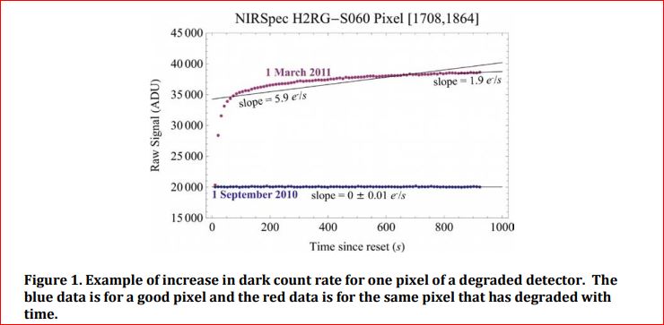
 < FIGURE 2
  < FIGURE 3
  < FIGURE 4
  FIGURE 5
  FIGURE 6
  < FIGURE 7
 < wHERE R = resistor and C = capacitor "


 hhhhhh Atomic Table Elements
![How Does a Spectrograph Work? [Infographic] - Scientific American](https://www.scientificamerican.com/media/inline/ancient-stars-how-does-spectrograph-work_2.jpg)
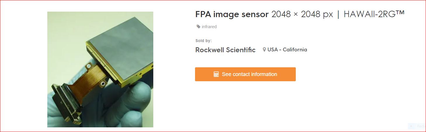
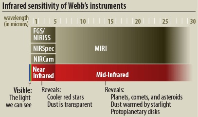

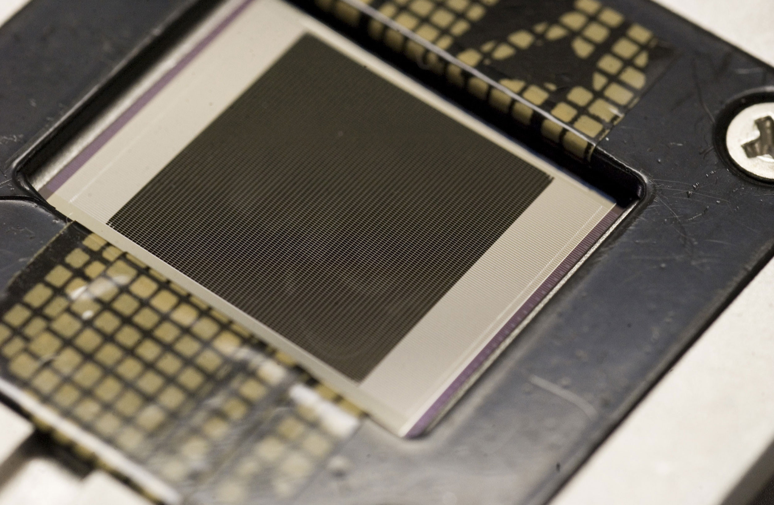


![Fig. 1. - (a) Wafer size comparison of a 300-mm SOI wafer with smaller-sized GaAs and SOI wafers. (b) The number of photonic components integrated on a single PIC over time for three photonic integration platforms [19].](https://ieeexplore.ieee.org/mediastore_new/IEEE/content/media/2944/9519571/9609553/xiang1-3126124-large.gif)
![Fig. 2. - Comparison of achieved waveguide loss for waveguide platforms compatible with heterogeneous integration. Propagation loss of 0.1 dB/m has been achieved in Si$_3$N$_4$ subject to high temperature annealing [9], while around 3 dB/m has been demonstrated within the thermal budget of heterogeneous integration using either a deuterated, low-temperature top-oxide-cladded single-mode Si$_3$N$_4$ waveguides [21], or multi-mode silicon waveguides [22].](https://ieeexplore.ieee.org/mediastore_new/IEEE/content/media/2944/9519571/9609553/xiang2-3126124-large.gif)
![Fig. 3. - (a) SEM image showing the III-V/Si gain section and its transition to passive Si loop mirror-based on-chip reflectors. Image also shows III-V/Si monitor PDs and Si edge-couplers for facet coupling. (b) Optical spectrum of a III-V/Si DFB laser with over 67 dB SMSR. Insets show the DFB array picture and SEM image of a Si $\lambda /4$-shift Bragg grating. (c) Device pictures and frequency noise comparison of heterogeneous III-V/Si E-DBR lasers and a hybrid RSOA-FBG laser [30].](https://ieeexplore.ieee.org/mediastore_new/IEEE/content/media/2944/9519571/9609553/xiang3-3126124-large.gif)
![Fig. 4. - (a) Device schematic design (top) and picture (bottom) of an 3-ring-based III-V/Si widely tunable laser. (b) Stacked optical spectra of the 3-ring-based III-V/Si widely tunable laser operating at different wavelengths (top). Bottom plots show the wavelength tuning map and associated laser SMSR map corresponding to different heater power values applied on the two Vernier rings [36].](https://ieeexplore.ieee.org/mediastore_new/IEEE/content/media/2944/9519571/9609553/xiang4-3126124-large.gif)
![Fig. 5. - (a) Schematic of the multilayer heterogeneous integration process. (b) Device design illustration of a III-V/Si/Si$_3$N$_4$ laser with Si$_3$N$_4$-based spiral grating. The inset IR images shows lasing within the Si$_3$N$_4$ cavity. (c) Cross-sectional SEM images showing the InP/Si gain and Si/Si$_3$N$_4$ section. (d) A comparison of temperature-dependent wavelength shift of the III-V/Si/Si$_3$N$_4$ laser and III-V/Si E-DBR laser [8].](https://ieeexplore.ieee.org/mediastore_new/IEEE/content/media/2944/9519571/9609553/xiang5-3126124-large.gif)
![Fig. 6. - (a) Device schematic of a GaAs/Si QD DFB laser in different configurations (I-III) and device cross-sectional SEM image and transmission electron microscopy image of the MOS (metal oxide semiconductor) capacitor, MOSCAP (IV-V). (b) Temperature-dependent light-current-voltage characteristic of the GaAs/Si QD DFB laser shown in a, and its spectral map up to 50 mA injection current at 20°C and 60°C, respectively [50]. (c) Small-signal modulation responses (left) and frequency noise spectrum (right) of a high-speed GaAs/Si QD DFB laser [51].](https://ieeexplore.ieee.org/mediastore_new/IEEE/content/media/2944/9519571/9609553/xiang6-3126124-large.gif)
![Fig. 7. - (a) Schematic of an InP/Si QW mode-locked laser (left), pulse width mapping as a function of the gain section forward bias current and SA section reverse voltage under passive mode locking state (middle) and single pulse autocorrelation trace with sech$^2$ fit (right) [55]. (b) Optical spectrum of QD-based III-V/Si comb laser (left). The flat spectrum reduces the need for channel equalization at the receiver; Eye diagram and BER of each channel from the device in a after external modulation at 10 Gb/s (right) [56].](https://ieeexplore.ieee.org/mediastore_new/IEEE/content/media/2944/9519571/9609553/xiang7-3126124-large.gif)
![Fig. 8. - (a) Device schematic and (b) images of laser soliton microcomb devices based on InP/Si/Si$_3$N$_4$ multilayer structure. (c) Optical spectrum of the generated 100 GHz-repetition rate single soliton state [29].](https://ieeexplore.ieee.org/mediastore_new/IEEE/content/media/2944/9519571/9609553/xiang8-3126124-large.gif)
![Fig. 9. - (a) Configuration of a III-V/Si OPA system with a $1 \times N$ star coupler, III-V/Si phase shifter array with a pitch of 4 $\mu$m, and grating emitter array. Right panel: schematic cross-section of the III-V/Si phase shifter array with locally opened n/p contact for probing one shifter on top. (b) Images of a fully fabricated 240-channel (upper panel) and 32-channel (lower panel) OPAs with enlarged SEM images for different parts of the OPA. (c) Measured beam profiles at 1550 nm wavelength with the beam steering across the field of view in the $\Psi$-axis at a 2.8° increment in the 32-channel OPA. The right inset shows the IR images of the main beam when steered by phase in $\Psi$-axis. (d) Measured beam profiles along $\theta$ axis ($\Psi$ = 0) with the beam steering when tuning the wavelength from 1450 nm to 1650 nm at a 10 nm increment. The top inset shows the IR images of the main beam when tuning wavelength in $\theta$-axis [77].](https://ieeexplore.ieee.org/mediastore_new/IEEE/content/media/2944/9519571/9609553/xiang9-3126124-large.gif)
![Fig. 10. - (a) Architecture of a low power consumption transceiver using QD-MLL sources and integrated linear ring modulator arrays for an 1-Tb/s link. (b) Image showing the 3D flip-chip bonded EIC and PIC (left). The SEM image on the right shows the densely-spaced copper pillar bumps for the 3D EIC-PIC integration [67].](https://ieeexplore.ieee.org/mediastore_new/IEEE/content/media/2944/9519571/9609553/xiang10-3126124-large.gif)

![Fig. 12. - (a) Semiconductor laser linewidth progression for three different integration approaches [19]. (b) Frequency noise comparison between a commercial ECDL (turquoise), a heterogeneous III-V/Si widely tunable laser (green) and a hybrid-integrated III-V/SiN laser based on SIL (blue). The green and blue curves correspond to the Si-Ring and SiN-SIL data shown in a, respectively [9], [34]. SIL stands for self-injection locking.](https://ieeexplore.ieee.org/mediastore_new/IEEE/content/media/2944/9519571/9609553/xiang12-3126124-large.gif)
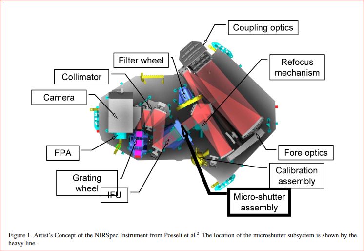
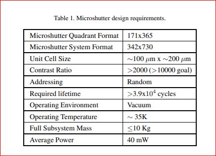
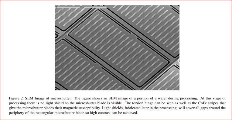 MSA-FIELD-SELECTOR-02.JPG
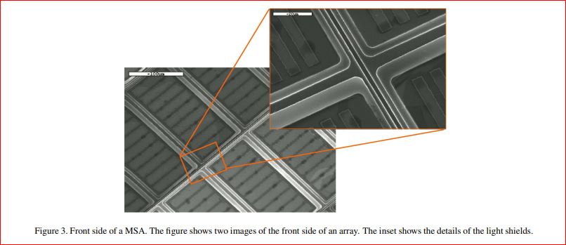
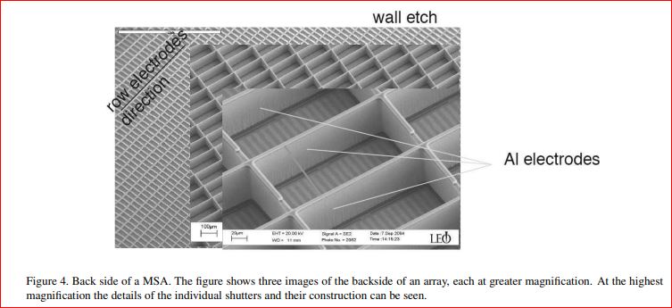 MSA-FIELD-SELECTOR-04.JPG
  MSA-FIELD-SELECTOR-05.JPG
 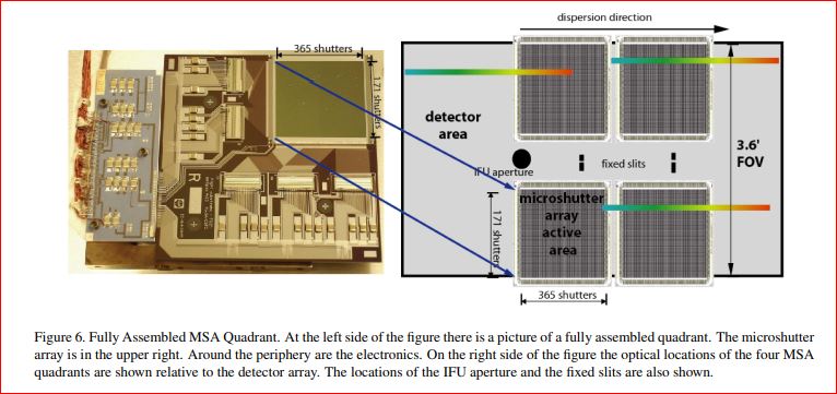 MSA-FIELD-SELECTOR-06.JPG
 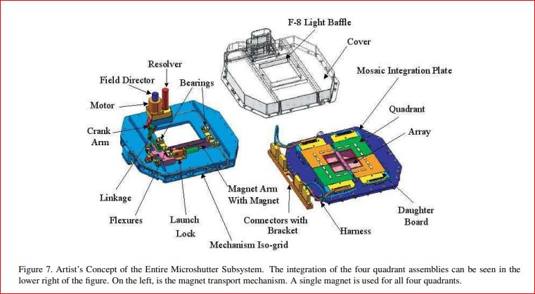 MSA-FIELD-SELECTOR-07.JPG
  MSA-FIELD-SELECTOR-REFERENCES.JPG
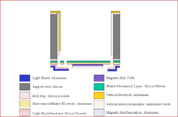
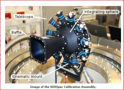
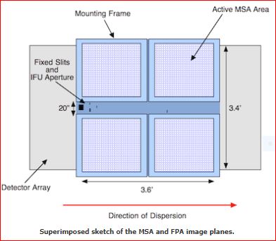 MSA = Micro shutter Array , FPA = Focal Plane Assembly
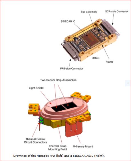
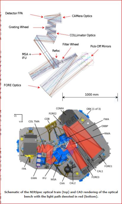
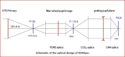
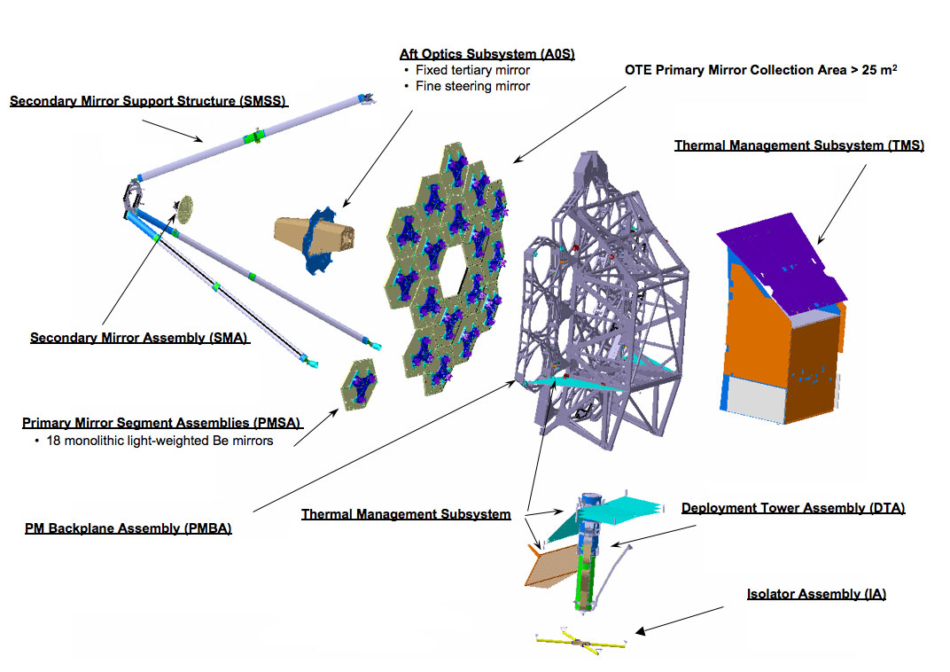
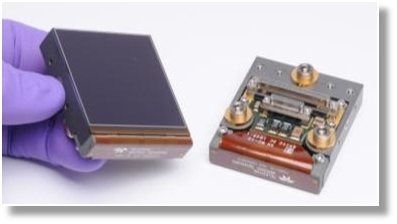 ( http://www.teledyne-si.com/products-and-services/imaging-sensors/hawaii-4rg )
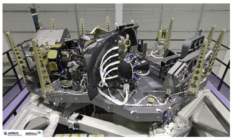
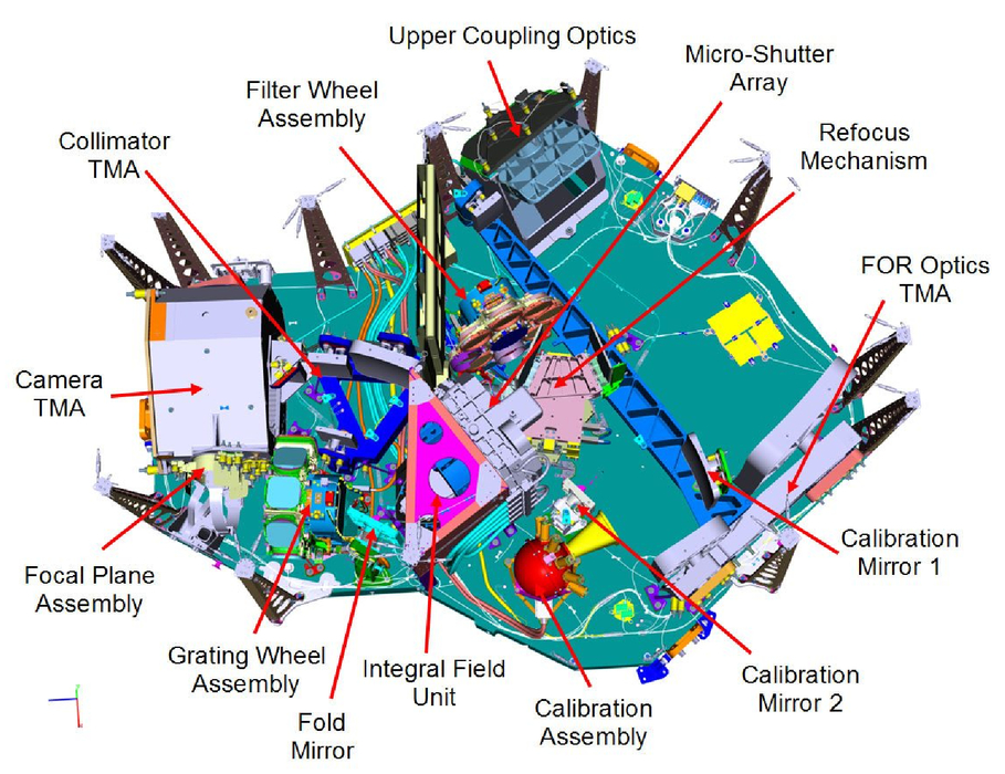
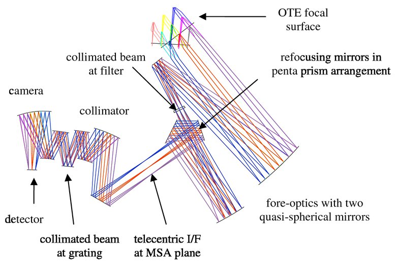
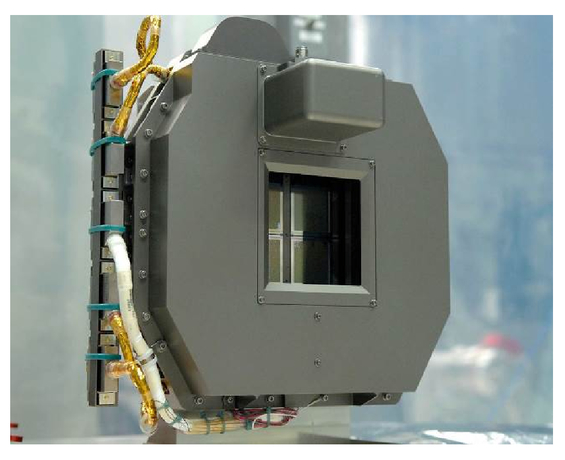
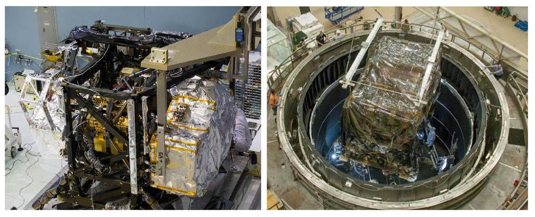
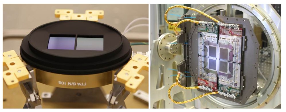
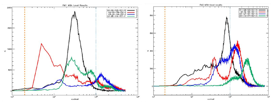
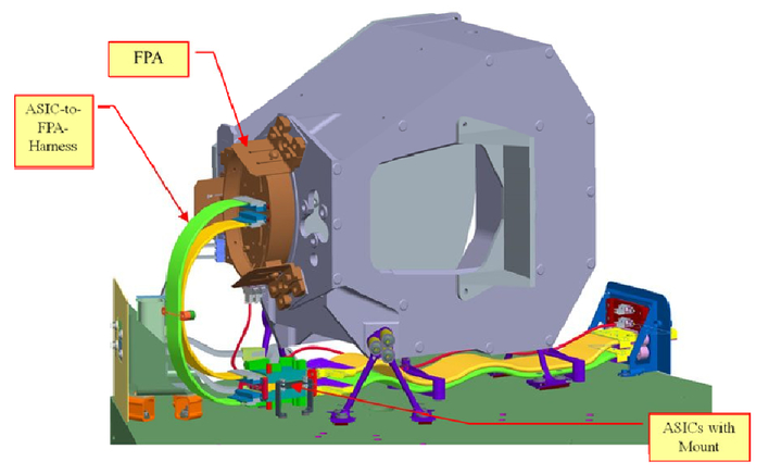
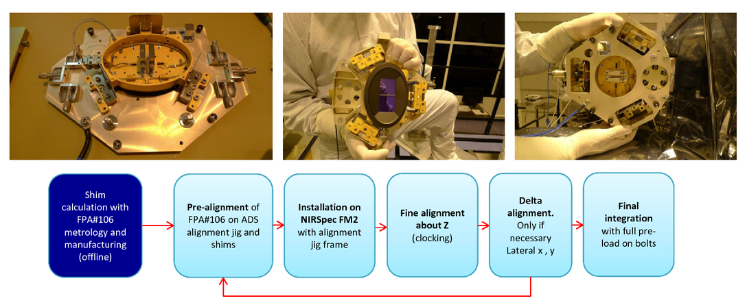
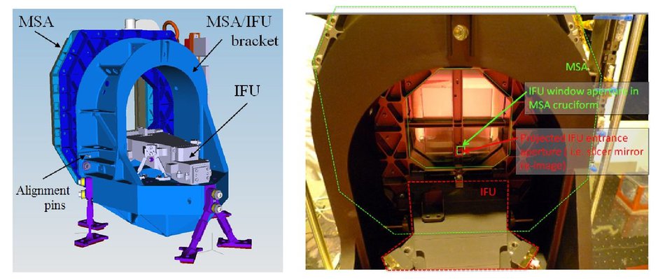
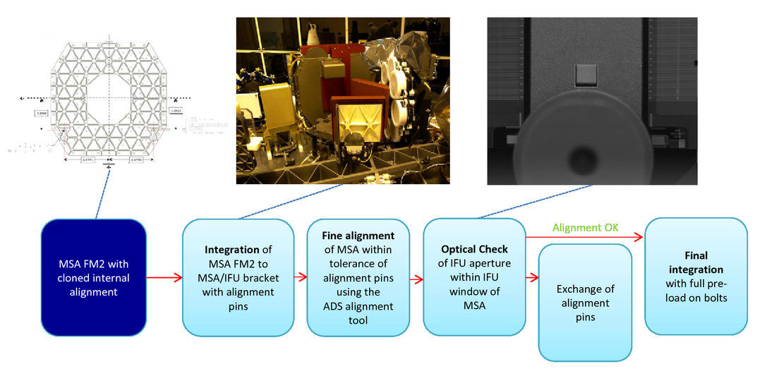


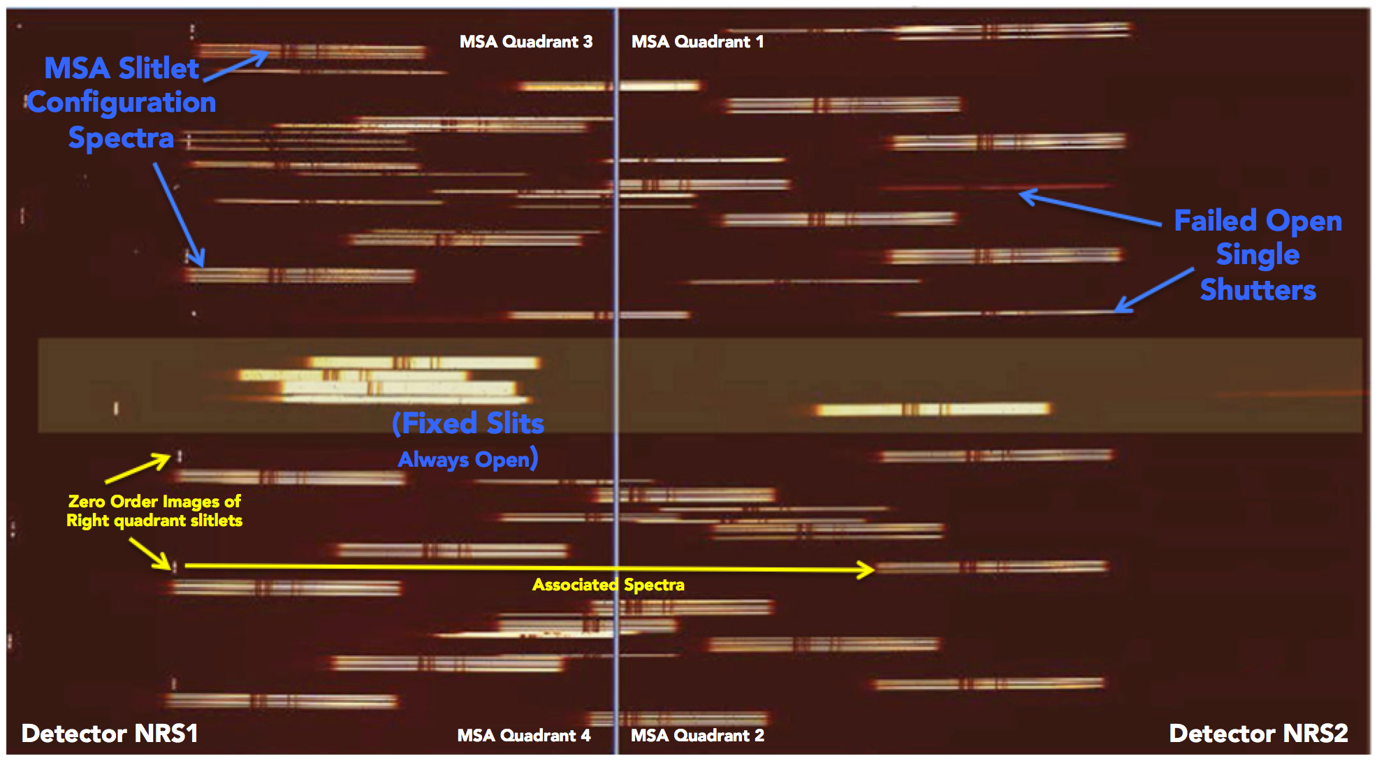